Patent Applications published on Nov 27, 2014
Explore the 6,992 U.S. Patent Applications published on the 48th week of 2014, including 4,825 applications that subsequently received a Patent Grant.
Featured patent applications from Nov 27, 2014
US20140346214A1
Human necessities
Surgical instruments employing sensors
According to an aspect of the present disclosure, a surgical instrument for operating on tissue is provided. The surgical instrument includes an end effector including a first tissue engaging member and a second tissue engaging member in juxtaposed relation to the first tissue engaging member; a gap determination element operatively associated with each of the first tissue engaging member and the second tissue engaging member for measuring a gap distance between the first tissue engaging member and the second tissue engaging member; and a tissue contact determining element operatively associated with a respective tissue contacting surface of at least one of the first tissue engaging member and the second tissue engaging member. The present disclosure also relates to methods of using the surgical instrument.
Published: 2014-11-27 Assignee: Smith& Nephew, Inc..US20140350562A1
Human necessities
Surgical aimer
The present disclosure relates to a surgical aimer including a shaft having a proximal portion and a distal portion and a handle coupled to the proximal portion of the shaft. The handle includes a mechanism for coupling the shaft to the handle and releasing the shaft from the handle.
Published: 2014-11-27 Assignee: ASM IP Holding B.V..US20140346650A1
Electricity
Systems and methods for thin-film deposition of metal oxides using excited nitrogen-oxygen species
The present invention relates to a process and system for depositing a thin film onto a substrate. One aspect of the invention is depositing a thin film metal oxide layer using atomic layer deposition (ALD).
Published: 2014-11-27 Assignee: INTERAXON INC..US20140347265A1
Physics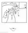
Wearable computing apparatus and method
A method is provided, performed by a wearable computing device comprising at least one bio-signal measuring sensor, the at least one bio-signal measuring sensor including at least one brainwave sensor, comprising: acquiring at least one bio-signal measurement from a user using the at least one bio-signal measuring sensor, the at least one bio-signal measurement comprising at least one brainwave state measurement; processing the at least one bio-signal measurement, including at least the at least one brainwave state measurement, in accordance with a profile associated with the user; determining a correspondence between the processed at least one bio-signal measurement and at least one predefined device control action; and in accordance with the correspondence determination, controlling operation of at least one component of the wearable computing device, such as modifying content displayed on a display of the wearable computing device. Various types of bio-signals, including brainwaves, may be measured and used to control the device in various ways.
Published: 2014-11-27 Assignee: ASM IP Holding B.V..US20140345644A1
Electricity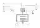
Method for cleaning reaction chamber using pre-cleaning process
A method for cleaning a reaction chamber is conducted after depositing an oxide, nitride, or oxynitride film on a substrate in a reaction chamber having interior surfaces on which oxide, nitride, or oxynitride is accumulated as a result of the deposition, said oxide, nitride, or oxynitride being selected from the group consisting of silicon oxide, silicon nitride, silicon oxynitride, metal oxide, metal nitride, and metal oxynitride. The method includes: oxidizing or nitriding the oxide, nitride, or oxynitride is accumulated on the interior surfaces of the reaction chamber, by RF-excited plasma of an oxygen- or nitrogen-containing gas in the absence of halide gas as a pre-cleaning step; and cleaning the interior surfaces of the reaction chamber, by RF-excited plasma of a halide cleaning gas.
Published: 2014-11-27 Assignee: ASM IP Holding B.V..US20140349033A1
Chemistry; metallurgy
Method for forming film by plasma-assisted deposition using two-frequency combined pulsed RF power
A method for forming a dielectric film on a substrate by plasma-assisted deposition, includes: introducing a Si-containing process gas to a reaction space wherein a substrate having a surface with patterned recesses is placed; and applying RF power to the process gas in the reaction space to form a dielectric film on the surface by plasma reaction. The RF power is comprised of pulses of high-frequency RF power and pulses of low-frequency RF power, which overlap and are synchronized.
Published: 2014-11-27 Assignee: VALEO SYSTEMES THERMIQUES.US20140346860A1
Electricity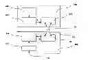
INDUCTIVE POWER TRANSMISSION DEVICE
The invention relates to a single device (500) combining the functions of an inductive power transmitter for recharging a mobile device and of near-field data communication (NFC) with said mobile device. Said device comprises at least the following elements: a) an inductive power transmission module (500) for transmitting power to a mobile device (600), including: a power transmission coil (110); a first device (120) for communicating between the power transmission module and the mobile device; and a device (130) for monitoring the charge of the mobile device; b) a second near-field communication device including: a data transmission coil (310); a second device (320) for communicating between the data transmission module and the mobile device; and a device (330) for controlling the exchanges of information with the mobile device; and c) a base (502) for receiving the mobile device.
Published: 2014-11-27 Assignee: HGST NETHERLANDS B.V..US20140346142A1
Chemistry; metallurgy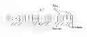
Method for making a chemical contrast pattern using block copolymers and sequential infiltration synthesis
A method for making a chemical contrast pattern uses directed self-assembly of block copolymers (BCPs) and sequential infiltration synthesis (SIS) of an inorganic material. For an example with poly(styrene-block-methyl methacrylate) (PS-b-PMMA) as the BCP and alumina as the inorganic material, the PS and PMMA self-assemble on a suitable substrate. The PMMA is removed and the PS is oxidized. A surface modification polymer (SMP) is deposited on the oxidized PS and the exposed substrate and the SMP not bound to the substrate is removed. The structure is placed in an atomic layer deposition chamber. Alumina precursors reactive with the oxidized PS are introduced and infuse by SIS into the oxidized PS, thereby forming on the substrate a chemical contrast pattern of SMP and alumina. The resulting chemical contrast pattern can be used for lithographic masks, for example to etch the underlying substrate to make an imprint template.
Published: 2014-11-27 Assignee: TOKYO ELECTRON LIMITED.US20140349032A1
Chemistry; metallurgy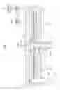
Film deposition method
A film deposition method, in which a film of a reaction product of a first reaction gas, which tends to be adsorbed onto hydroxyl radicals, and a second reaction gas capable of reacting with the first reaction gas is formed on a substrate provided with a concave portion, includes a step of controlling an adsorption distribution of the hydroxyl radicals in a depth direction in the concave portion of the substrate; a step of supplying the first reaction gas on the substrate onto which the hydroxyl radicals are adsorbed; and a step of supplying the second reaction gas on the substrate onto which the first reaction gas is adsorbed.
Published: 2014-11-27 Assignee: METROLOGIC INSTRUMENTS, INC..US20140346233A1
Physics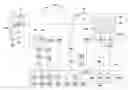
Imaging based barcode scanner engine with multiple elements supported on a common printed circuit board
An apparatus for use in decoding a bar code symbol may include an image sensor integrated circuit having a plurality of pixels, timing and control circuitry for controlling an image sensor, gain circuitry for controlling gain, and analog to digital conversion circuitry for conversion of an analog signal to a digital signal. The apparatus may also include a printed circuit board for receiving the image sensor integrated circuit. The connection between the image sensor integrated circuit and the printed circuit board characterized by a plurality of conductive adhesive connectors disposed between a plurality of electrode pads and a plurality of contact pads, where the conductive adhesive connectors provide electrical input/output and mechanical connections between the image sensor integrated circuit and the printed circuit board. The apparatus may be operative for processing image signals generated by the image sensor integrated circuit for attempting to decode the bar code symbol.