Patent Applications published on Jul 5, 2018
Explore the 8,001 U.S. Patent Applications published on the 27th week of 2018, including 6,158 applications that subsequently received a Patent Grant.
Featured patent applications from Jul 5, 2018
US20180189923A1
Physics
Draw call visibility stream
This disclosure describes a device configured to generate a primitive visibility stream that indicates whether respective primitives of a set of primitives are visible when rendered and to generate, based on the primitive visibility stream, a draw call visibility stream that indicates whether respective draw calls for rendering the set of primitives include instructions for rendering visible primitives of the set of primitives. Based on the draw call visibility stream indicating that a respective draw call does not include instructions for rendering visible primitives, the device is further configured to drop the respective draw call. Based on the draw call visibility stream indicating that the respective draw call includes instructions for rendering visible primitives, the device is further configured to execute the respective draw call.
Published: 2018-07-05 Assignee: Nok Nok Labs, Inc..US20180191501A1
Electricity
System and method for sharing keys across authenticators
A system, apparatus, method, and machine readable medium are described for sharing authentication data. For example, one embodiment of a method comprises: generating and storing a persistent group identification code (Group-ID) for a group of authenticators sharing a common set of authorization (Uauth) keys, an initial Group-ID to be generated on a first use of a first authenticator and/or following a factory reset of the first authenticator generating and storing an individual asymmetric wrapping key encryption key (WKEK) on a first use of the first authenticator and/or following each factory reset of the first authenticator; generating and storing a symmetric wrapping key (WK), the wrapping key to be generated on a first use of the first authenticator and/or following each factory reset of the first authenticator; generating a join-block using an authenticator identification code for the first authenticator and the WKEK, the join-block usable to join an existing authenticator group, the join block to be sent to a second authenticator; verifying the join-block at the second authenticator and generating a join response block responsive to user approval, the join response block generated by encrypting the WK and Group-ID using the WKEK, the join response block to be transmitted to the first authenticator; and decrypting the join response block and storing the WK and Group-ID.
Published: 2018-07-05 Assignee: HITACHI KOKUSAI ELECTRIC INC., KOKUSAI ELECTRIC CORPORATION.US20180190496A1
Electricity
Method of manufacturing semiconductor device, substrate processing apparatus, recording medium, and supply system
A method of manufacturing a semiconductor device, includes: forming a film on a substrate by performing a cycle a predetermined number of times, the cycle including: supplying two or more kinds of halogen-based precursors having the same major elements and different halogen elements, or different major elements and the same halogen elements, or different major elements and different halogen elements to the substrate while overlapping at least portions of supply periods of the two or more kinds of halogen-based precursors; and supplying a reactant having a chemical structure different from chemical structures of the two or more kinds of halogen-based precursors to the substrate.
Published: 2018-07-05 Assignee: L'Air Liquide Societe Anonyme Pour L'Etude Et L'Exploitation Des Procedes Georges Claude.US20180187303A1
Chemistry; metallurgy
LANTHANIDE PRECURSORS AND DEPOSITION OF LANTHANIDE-CONTAINING FILMS USING THE SAME
Lanthanide-containing film forming compositions comprising Lanthanide precursors having the general formulae:
Published: 2018-07-05 Assignee: MASIMO CORPORATION.US20180184917A1
Human necessities
Patient monitor for monitoring microcirculation
A patient monitor capable of measuring microcirculation at a tissue site includes a light source, a beam splitter, a photodetector and a patient monitor. Light emitted from the light source is split into a reference arm and a sample arm. The light in the sample arm is directed at a tissue site, such as an eyelid. The reflected light from the tissue site is interfered with the light from the reference arm. The photodetector measures the interference of the light from both the sample arm and the reference arm. The patient monitor uses the measurements from the photodetector to calculate the oxygen saturation at the tissue site and monitor the microcirculation at the tissue site.
Published: 2018-07-05 Assignee: FMR LLC.US20180191503A1
Electricity
Asynchronous Crypto Asset Transfer and Social Aggregating, Fractionally Efficient Transfer Guidance, Conditional Triggered Transaction, Datastructures, Apparatuses, Methods and Systems
The Asynchronous Crypto Asset Transfer and Social Aggregating, Fractionally Efficient Transfer Guidance, Conditional Triggered Transaction, Datastructures, Apparatuses, Methods and Systems (“SOCOACT”) transforms transfer of assets (TOA) initiation request inputs via SOCOACT components into TOA confirmation outputs. A crypto asset transfer notification is sent to a first entity from a second entity. Account verification data generated by the second entity is determined. A set of account data stored by the first entity is retrieved and used to generate a hash. It is verified that the determined account verification data matches the generated hash. A requested asset is determined. An API call to generate a crypto token asset for the requested asset in a socially aggregated blockchain datastructure is made. An address of an aggregated crypto transaction trigger entry is determined. Oracle data that satisfies the crypto smart rule is provided.
Published: 2018-07-05 Assignee: ASM IP Holding B.V..US20180190486A1
Electricity
Formation of SiOCN thin films
Methods for depositing silicon oxycarbonitride (SiOCN) thin films on a substrate in a reaction space are provided. The methods can include at least one plasma enhanced atomic layer deposition (PEALD) cycle including alternately and sequentially contacting the substrate with a silicon precursor and a second reactant that does not include oxygen. In some embodiments the methods allow for the deposition of SiOCN films having improved acid-based wet etch resistance.
Published: 2018-07-05 Assignee: C3.ai, Inc..US20180191867A1
Electricity
Systems, methods, and devices for an enterprise AI and internet-of-things platform
Systems, methods, and devices for a cyberphysical (IoT) software application development platform based upon a model driven architecture and derivative IoT SaaS applications are disclosed herein. The system may include concentrators to receive and forward time-series data from sensors or smart devices. The system may include message decoders to receive messages comprising the time-series data and storing the messages on message queues. The system may include a persistence component to store the time-series data in a key-value store and store the relational data in a relational database. The system may include a data services component to implement a type layer over data stores. The system may also include a processing component to access and process data in the data stores via the type layer, the processing component comprising a batch processing component and an iterative processing component.
Published: 2018-07-05 Assignee: WIN SEMICONDUCTORS CORP..US20180191322A1
Electricity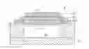
Method for fabricating bulk acoustic wave resonator with mass adjustment structure
A method for fabricating bulk acoustic wave resonator with mass adjustment structure, comprising following steps of: forming a sacrificial structure mesa on a substrate; etching the sacrificial structure mesa such that any two adjacent parts have different heights, a top surface of a highest part of the sacrificial structure mesa is coincident with a mesa top extending plane; forming an insulating layer on the sacrificial structure mesa and the substrate; polishing the insulating layer to form a polished surface; forming a bulk acoustic wave resonance structure including a top electrode, a piezoelectric layer and a bottom electrode on the polished surface; etching the sacrificial structure mesa to form a cavity; the insulating layer between the polished surface and the mesa top extending plane forms a frequency tuning structure, the insulating layer between the mesa top extending plane and the cavity forms a mass adjustment structure.
Published: 2018-07-05 Assignee: ADEIA SEMICONDUCTOR BONDING TECHNOLOGIES INC..US20180190580A1
Electricity
Bonded structures with integrated passive component
In various embodiments, a bonded structure is disclosed. The bonded structure can include an element and a passive electronic component having a first surface bonded to the element and a second surface opposite the first surface. The passive electronic component can comprise a first anode terminal bonded to a corresponding second anode terminal of the element and a first cathode terminal bonded to a corresponding second cathode terminal of the element. The first anode terminal and the first cathode terminal can be disposed on the first surface of the passive electronic component.