Patent Applications published on Jan 24, 2019
Explore the 7,958 U.S. Patent Applications published on the 04th week of 2019, including 6,175 applications that subsequently received a Patent Grant.
Featured patent applications from Jan 24, 2019
US20190021733A1
Human necessities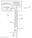
End effector with redundant closing mechanisms
End effectors with redundant closing mechanisms, and related tools and methods are disclosed. The disclosed end effectors may be particularly beneficial when used for minimally invasive surgery. An example surgical tool comprises an elongate shaft having a proximal end and a distal end, a tool body disposed at the distal end of the shaft, a jaw movable relative to the tool body between a clamped configuration and an open configuration, a first actuation mechanism coupled with the jaw and operable to vary the position of the jaw relative to the tool body between the clamped configuration and the open configuration, and a second actuation mechanism coupled with the jaw. The second actuation mechanism has a first configuration where the jaw is held in the clamped configuration and a second configuration where the position of the jaw relative to the tool body is unconstrained by the second actuation mechanism.
Published: 2019-01-24 Assignee: ASM IP Holding B.V..US20190027583A1
Electricity
Method for depositing a group IV semiconductor and related semiconductor device structures
A method for depositing a Group IV semiconductor is disclosed. The method may include, providing a substrate within a reaction chamber and heating the substrate to a deposition temperature. The methods may further include, exposing the substrate to at least one Group IV precursor and exposing the substrate to at least one Group IIIA metalorganic dopant precursor. The methods may further include depositing a Group IV semiconductor on a surface of the substrate. Semiconductor device structures including a Group IV semiconductor deposited by the methods of the disclosure are also provided.
Published: 2019-01-24 Assignee: ASM IP Holding B.V..US20190027573A1
Electricity
Methods for forming a semiconductor device structure and related semiconductor device structures
Methods for forming a semiconductor device structure are provided. The methods may include forming a molybdenum nitride film on a substrate by atomic layer deposition by contacting the substrate with a first vapor phase reactant comprising a molybdenum halide precursor, contacting the substrate with a second vapor phase reactant comprise a nitrogen precursor, and contacting the substrate with a third vapor phase reactant comprising a reducing precursor. The methods provided may also include forming a gate electrode structure comprising the molybdenum nitride film, the gate electrode structure having an effective work function greater than approximately 5.0 eV. Semiconductor device structures including molybdenum nitride films are also provided.
Published: 2019-01-24 Assignee: ASM IP Holding B.V..US20190027605A1
Electricity
Method for depositing a group IV semiconductor and related semiconductor device structures
A method for depositing a Group IV semiconductor on a surface of a substrate is disclosed. The method may include: providing a substrate within a reaction chamber and heating the substrate to a deposition temperature. The methods may further include: exposing the substrate to at least one Group IV precursor and exposing the substrate to at least one Group IIIA dopant precursor; wherein the at least one Group IIIA dopant precursor comprises a borohydride, an organic borohydride, a halide, or an organohalide. Semiconductor device structures including a Group IV semiconductor deposited by the methods of the disclosure are also provided.
Published: 2019-01-24 Assignee: ASM IP Holding B.V..US20190027584A1
Electricity
Method for selectively depositing a Group IV semiconductor and related semiconductor device structures
A method for selectively depositing a Group IV semiconductor on a surface of a substrate is disclosed. The method may include, providing a substrate within a reaction chamber and heating the substrate to a deposition temperature. The method may further include, exposing the substrate to at least one Group IV precursor, and exposing the substrate to at least one Group IIIA halide dopant precursor. Semiconductor device structures including a Group IV semiconductor deposited by the methods of the disclosure are also provided.
Published: 2019-01-24 Assignee: Rosemount Aerospace Inc..US20190029121A1
Electricity
BGA component masking dam and a method of manufacturing with the BGA component masking dam
The proposed masking dam protects ball grid array integrated circuit components from conformal coating overflow, preventing joint breakage and thermal mismatch. The masking dam includes a frame with an integrated seal, a cover, and a fastening mechanism. The frame is sealed to a circuit board surround a component, the cover is attached to the frame, and the masking dam is secured to protect the component.
Published: 2019-01-24 Assignee: Matterport, Inc..US20190026956A1
Physics
Employing three-dimensional (3D) data predicted from two-dimensional (2D) images using neural networks for 3D modeling applications and other applications
The disclosed subject matter is directed to employing machine learning models configured to predict 3D data from 2D images using deep learning techniques to derive 3D data for the 2D images. In some embodiments, a system is described comprising a memory that stores computer executable components, and a processor that executes the computer executable components stored in the memory. The computer executable components comprise a reception component configured to receive two-dimensional images, and a three-dimensional data derivation component configured to employ one or more three-dimensional data from two-dimensional data (3D-from-2D) neural network models to derive three-dimensional data for the two-dimensional images.
Published: 2019-01-24 Assignee: MASIMO CORPORATION.US20190021638A1
Human necessities
System and method for monitoring the life of a physiological sensor
Aspects of the present disclosure include a sensor configured to store in memory indications of sensor use information and formulas or indications of formulas for determining the useful life of a sensor from the indications of sensor use information. A monitor connected to the sensor monitors sensor use and stores indications of the use on sensor memory. The monitor and/or sensor compute the useful life of the sensor from the indications of use and the formulas. When the useful life of the sensor is reached, an indication is given to replace the sensor.
Published: 2019-01-24 Assignee: CISCO TECHNOLOGY, INC..US20190028552A1
Electricity
Managing a distributed network of function execution environments
Systems, methods, and computer-readable media for managing a distributed network of function execution environments. In some examples, a function router registers a plurality of execution endpoints on a catalog of execution endpoints and functions, each of the plurality of execution endpoints including a respective runtime environment capable of executing one or more functions. The function router receives, from a client, a request to execute a particular function and, based on the request, queries the catalog for the particular function and execution endpoints associated with the particular function. The function router receives a query response identifying one or more execution endpoints associated with the particular function, and selects an execution endpoint for executing the particular function based on one or more criteria associated with the request. The function router then sends to the client a response identifying the execution endpoint selected for executing the particular function.
Published: 2019-01-24 Assignee: TOSHIBE TEC KABUSHIKI KAISHA.US20190028598A1
Electricity
Information processing apparatus configured to block inputs from an operation panel when the operation panel is swiveled
An information processing apparatus includes a casing, a cover that is movable to an open position to provide access to an interior of the casing, an operation panel configured to receive an input operation and mounted on the casing to be movable between a first position at which the operation panel interferes with the opening of the cover and a second position at which the operation panel does not interfere with the opening of the cover, and a control unit including a processor that is configured to block any input operation received by the operation unit when the operation panel moves to the second position.