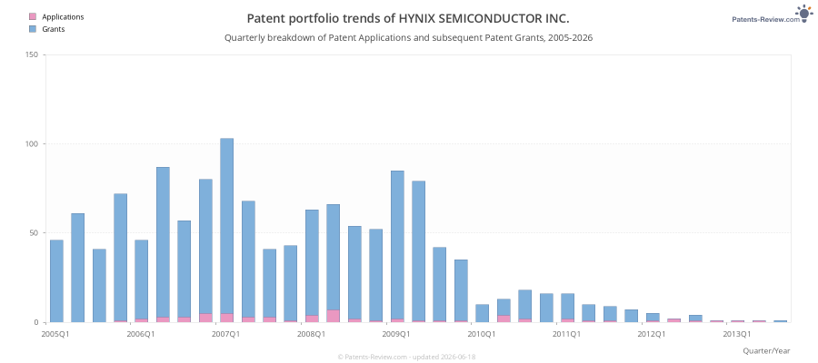
HYNIX SEMICONDUCTOR INC.
Kyoungki-do
South Korea
1,335
2013-07-18
1,273
2015-01-06
Top Inventors for applications by HYNIX SEMICONDUCTOR INC.
These are the the leading inventors for applications assigned to HYNIX SEMICONDUCTOR INC.:
- Hee Bok KANG 37 Chungcheongbuk-do, South Korea
- Suk Kyoung HONG 25 Gyeonggi-do, South Korea
- Heon Yong CHANG 21 Gyeonggi-do, South Korea
- Chang-Ho DO 19 Kyoungki-do, South Korea
- Heon Yong CHANG 16 Kyoungki-do, South Korea
- Min Suk SUH 16 Seoul, South Korea
- Hyun Woo LEE 14 Kyoungki-do, South Korea
- Kyung-Hoon KIM 13 Kyoungki-do, South Korea
- Ji-Eun JANG 12 Kyoungki-do, South Korea
- Jung Geun KIM 12 Seoul, South Korea
- Seung Taek YANG 12 Seoul, South Korea
- Kwon Whan HAN 12 Seoul, South Korea
- Chang-Ho DO 11 Ichon-shi, South Korea
- Hoon CHOI 11 Kyoungki-do, South Korea
- Chang-Hyuk Lee 11 Kyoungki-do, South Korea
- Ki-Won NAM 11 Kyoungki-do, South Korea
- Soo Hyun Kim 11 Seoul, South Korea
- Kee-Teok Park 11 Kyoungki-do, South Korea
- Qwan Ho CHUNG 11 Gyeonggi-do, South Korea
- Sung-min Kim 10 Seoul, South Korea
- BEOM-JU SHIN 10 Kyoungki-do, South Korea
- Sung-Kwon Lee 10 Kyoungki-do, South Korea
- Sung-Kwon LEE 10 Ichon-shi, South Korea
- Jong Hoon KIM 9 Gyeonggi-do, South Korea
- Jun Gi Choi 9 Ichon-shi, South Korea
- Chun-Seok JEONG 9 Kyoungki-do, South Korea
- Ki-Ho KIM 9 Kyoungki-do, South Korea
- Geun-Il Lee 9 Kyoungki-do, South Korea
- Nak Kyu PARK 8 Kyoungki-do, South Korea
- Kang Seol Lee 8 Ichon-shi, South Korea
- Nak Heon Choi 8 Kyoungki-do, South Korea
- Ho-Youb CHO 8 Kyoungki-do, South Korea
- Jae-Jin Lee 8 Kyoungki-do, South Korea
- Jae-Hyuk IM 8 Kyoungki-do, South Korea
- Seong Cheol KIM 8 Gyeongsangnam-do, South Korea
- Sang Tae AHN 8 Kyoungki-do, South Korea
- Khil-Ohk KANG 8 Kyoungki-do, South Korea
- Jun-Gi CHOI 8 Kyoungki-do, South Korea
- Sang-Jin BYEON 8 Kyoungki-do, South Korea
- Seok Pyo SONG 8 Seoul, South Korea
- Hee Bok KANG 7 Daejeon, South Korea
- Hwang HUR 7 Kyoungki-do, South Korea
- Kyung-Whan KIM 7 Kyoungki-do, South Korea
- Jeong Tae KIM 7 Kyoungki-do, South Korea
- Young Jin LEE 7 Kyoungki-do, South Korea
- Ji-Hyun KIM 7 Seoul, South Korea
- Kyung Do KIM 7 Seoul, South Korea
- Dong Ha JUNG 7 Kyoungki-do, South Korea
- Baek Mann KIM 7 Kyoungki-do, South Korea
- Geun Su Lee 7 Kyoungki-do, South Korea
- Young Jun NAM 7 Kwangju, South Korea
- Kyoung-Nam KIM 7 Kyoungki-do, South Korea
- Dong Sun SHEEN 7 Kyoungki-do, South Korea
- Hae Chan PARK 7 Seoul, South Korea
- Jin-Hong Ahn 7 Ichon-shi, South Korea
- Kwang Jun CHO 7 Seoul, South Korea
- Hyun Chul SOHN 7 Seoul, South Korea
- Hi-Hyun Han 6 Kyoungki-do, South Korea
- Dong Kyun Lee 6 Seoul, South Korea
- Yong-Bok An 6 Kyoungki-do, South Korea
- Jae-Chang Jung 6 Kyoungki-do, South Korea
- Jae Chang Jung 6 Seoul, South Korea
- Seok-Cheol Yoon 6 Kyoungki-do, South Korea
- Kook Whee Kwak 6 Kyoungki-do, South Korea
- Jee-Yul KIM 6 Kyoungki-do, South Korea
- Cheol Mo Jeong 6 Kyeongki-do, South Korea
- Dong-Keun Kim 6 Kyoungki-do, South Korea
- Chang Jun PARK 6 Gyeonggi-do, South Korea
- Ho-Uk Song 6 Kyoungki-do, South Korea
- Jin-Hong AN 6 Gyeonggi-do, South Korea
- Hee-Bok Kang 6 Ichon-shi, South Korea
- Kyung Hoon KIM 6 Ichon-shi, South Korea
- Jae-Boum PARK 6 Kyoungki-do, South Korea
- Kang-Seol LEE 6 Seoul, South Korea
- Chang Yeol LEE 6 Seoul, South Korea
- Suk Kyoung HONG 6 Kyoungki-do, South Korea
- Cheol Hwan Park 6 Seoul, South Korea
- Tae-Woo Jung 6 Kyoungki-do, South Korea
- Tae Min KANG 6 Seoul, South Korea
- Myung Geun PARK 6 Seoul, South Korea
- Ja Chun KU 5 Gyeonggi-do, South Korea
- Ho-Jin Cho 5 Kyoungki-do, South Korea
- Tae Hyeok Lee 5 Kyoungki-do, South Korea
- Seung-Hyun LEE 5 Gyeonggi-do, South Korea
- Sung-Kyu MIN 5 Seoul, South Korea
- Whee Won Cho 5 Chungcheongbuk-do, South Korea
- Tae Yun KIM 5 Chungcheongbuk-do, South Korea
- Sang Deok Kim 5 Seoul, South Korea
- Jin Yong SEONG 5 Seoul, South Korea
- Hyeon Ju AN 5 Kyoungki-do, South Korea
- Dong Ha Jung 5 Gyeonggi-do, South Korea
- Ki Soo Shin 5 Kyoungki-do, South Korea
- Kwang-Myoung RHO 5 Kyoungki-do, South Korea
- Young Jin Lee 5 Gyeonggi-do, South Korea
- Dong Uk LEE 5 Kyoungki-do, South Korea
- Seung-Min Oh 5 Kyoungki-do, South Korea
- Ky-Hyun Han 5 Kyoungki-do, South Korea
- Jung-Hoon Park 5 Seoul, South Korea
- Sang-Hee Kang 5 Kyoungki-do, South Korea
- Nam Kyeong Kim 5 Kyeongki-do, South Korea
Recent patent applications by HYNIX SEMICONDUCTOR INC.
HYNIX SEMICONDUCTOR INC. based in Kyoungki-do, KR has been assigned the rights to these inventions. The list includes both Pending Applications and Patent Grants:
US20130181761A1
ElectricityTrimming of operative parameters in electronic devices based on corrections mappings
#2 | 2013-04-11US20130087919A1
ElectricityLIGHTWEIGHT AND COMPACT THROUGH-SILICON VIA STACK PACKAGE WITH EXCELLENT ELECTRICAL CONNECTIONS AND METHOD FOR MANUFACTURING THE SAME
#3 | 2013-01-31US20130027076A1
ElectricityAPPARATUS FOR DETECTING PATTERN ALIGNMENT ERROR
#4 | 2012-12-20US20120322216A1
ElectricityMETHOD FOR REDUCING POLY-DEPLETION IN DUAL GATE CMOS FABRICATION PROCESS
#5 | 2012-09-13 ✅ Patent 8,507,665 granted on 2013-08-13US20120231635A1
ElectricityTemplate derivative for forming ultra-low dielectric layer and method of forming ultra-low dielectric layer using the same
#6 | 2012-09-13 ✅ Patent 8,354,350 granted on 2013-01-15US20120231634A1
ElectricityTemplate derivative for forming ultra-low dielectric layer and method of forming ultra-low dielectric layer using the same
#7 | 2012-08-30 ✅ Patent 8,441,116 granted on 2013-05-14US20120217637A1
ElectricitySemiconductor package having substrate for high speed semiconductor package
#8 | 2012-08-16US20120205802A1
ElectricityPRINTED CIRCUIT BOARD AND FLIP CHIP PACKAGE USING THE SAME WITH IMPROVED BUMP JOINT RELIABILITY
#9 | 2012-05-10US20120115278A1
ElectricitySTACKED SEMICONDUCTOR PACKAGE WITHOUT REDUCTION IN DATA STORAGE CAPACITY AND METHOD FOR MANUFACTURING THE SAME
#10 | 2012-04-12US20120088336A1
ElectricitySEMICONDUCTOR PACKAGE HAVING AN IMPROVED CONNECTION STRUCTURE AND METHOD FOR MANUFACTURING THE SAME
#11 | 2012-01-26 ✅ Patent 8,198,161 granted on 2012-06-12US20120021576A1
ElectricityVertical transistor and method for forming the same
#12 | 2012-01-19US20120013010A1
ElectricityBONDING PAD FOR ANTI-PEELING PROPERTY AND METHOD FOR FABRICATING THE SAME
#13 | 2012-01-12 ✅ Patent 8,394,717 granted on 2013-03-12US20120009775A1
ElectricitySemiconductor package with a reduced volume and thickness and capable of high speed operation and method for fabricating the same
#14 | 2012-01-12 ✅ Patent 8,422,283 granted on 2013-04-16US20120009758A1
ElectricityPhase change memory device to prevent thermal cross-talk and method for manufacturing the same
#15 | 2012-01-12 ✅ Patent 8,519,539 granted on 2013-08-27US20120007240A1
ElectricityMetal wire for a semiconductor device formed with a metal layer without voids therein and a method for forming the same
#16 | 2011-12-22 ✅ Patent 8,202,762 granted on 2012-06-19US20110312128A1
ElectricityStack package having reduced electrical connection length suitable for high speed operations and method of manufacturing the same
#17 | 2011-11-24 ✅ Patent 8,399,285 granted on 2013-03-19US20110287602A1
ElectricityPhase change memory device having a bent heater and method for manufacturing the same
#18 | 2011-11-10 ✅ Patent 8,148,764 granted on 2012-04-03US20110272784A1
ElectricitySemiconductor device having a high aspect cylindrical capacitor and method for fabricating the same
#19 | 2011-10-27 ✅ Patent 8,202,781 granted on 2012-06-19US20110263090A1
ElectricitySemiconductor device having vertical pillar transistors and method for manufacturing the same
#20 | 2011-10-20 ✅ Patent 8,114,733 granted on 2012-02-14US20110256696A1
ElectricitySemiconductor device for preventing the leaning of storage nodes and method for manufacturing the same
#21 | 2011-10-20 ✅ Patent 8,203,204 granted on 2012-06-19US20110254145A1
ElectricityStacked semiconductor package
#22 | 2011-10-06 ✅ Patent 8,247,878 granted on 2012-08-21US20110241107A1
ElectricitySemiconductor device and method of manufacturing the same
#23 | 2011-09-29US20110233795A1
ElectricitySTACKED WAFER LEVEL PACKAGE HAVING A REDUCED SIZE
#24 | 2011-09-29 ✅ Patent 8,338,951 granted on 2012-12-25US20110233781A1
ElectricityMetal line of semiconductor device having a diffusion barrier with an amorphous TaBN layer and method for forming the same
#25 | 2011-09-01 ✅ Patent 8,345,395 granted on 2013-01-01US20110211291A1
ElectricityElectrostatic discharge protection circuit having a reduced size and enhanced discharge
#26 | 2011-08-25 ✅ Patent 8,315,064 granted on 2012-11-20US20110203935A1
ElectricityApparatus for detecting pattern alignment error
#27 | 2011-08-18 ✅ Patent 8,218,384 granted on 2012-07-10US20110199849A1
PhysicsSense amplifier for controlling flip error and driving method thereof
#28 | 2011-08-18 ✅ Patent 8,232,654 granted on 2012-07-31US20110198722A1
ElectricitySemiconductor package through-electrode suitable for a stacked semiconductor package and semiconductor package having the same
#29 | 2011-07-21 ✅ Patent 8,322,626 granted on 2012-12-04US20110174886A1
ElectricityIntegrated circuit with embedded RFID
#30 | 2011-07-07 ✅ Patent 8,455,329 granted on 2013-06-04US20110165752A1
ElectricityPhase change memory device capable of increasing sensing margin and method for manufacturing the same
#31 | 2011-07-07 ✅ Patent 8,773,161 granted on 2014-07-08US20110163778A1
ElectricityImpedance calibration circuit, semiconductor memory device with the impedance calibration circuit and layout method of internal resistance in the impedance calibration circuit
#32 | 2011-06-09 ✅ Patent 8,293,650 granted on 2012-10-23US20110136316A1
ElectricityPhase change memory device in which a phase change layer is stably formed and prevented from lifting and method for manufacturing the same
#33 | 2011-06-09 ✅ Patent 8,373,234 granted on 2013-02-12US20110133283A1
ElectricitySemiconductor device and method for forming the same
#34 | 2011-06-02 ✅ Patent 8,051,344 granted on 2011-11-01US20110131457A1
PhysicsSemiconductor memory testing device and method of testing semiconductor using the same
#35 | 2011-06-02 ✅ Patent 8,447,571 granted on 2013-05-21US20110128067A1
ElectricityTrimming of operative parameters in electronic devices based on corrections mappings
#36 | 2011-06-02 ✅ Patent 8,203,217 granted on 2012-06-19US20110127672A1
ElectricitySemiconductor package having a stacked wafer level package and method for fabricating the same
#37 | 2011-05-12 ✅ Patent 8,189,411 granted on 2012-05-29US20110109362A1
PhysicsCircuit for controlling an enabling time of an internal control signal according to an operating frequency of a memory device and the method thereof
#38 | 2011-04-28US20110095352A1
ElectricityFLASH MEMORY DEVICE AND FABRICATION METHOD THEREOF
#39 | 2011-04-21 ✅ Patent 8,148,243 granted on 2012-04-03US20110092034A1
ElectricityZero capacitor RAM with reliable drain voltage application and method for manufacturing the same
#40 | 2011-04-21 ✅ Patent 8,399,355 granted on 2013-03-19US20110092024A1
ElectricityStacked semiconductor package and method for manufacturing the same
#41 | 2011-04-07 ✅ Patent 8,741,734 granted on 2014-06-03US20110079871A1
ElectricitySemiconductor device and method of fabricating the same
#42 | 2011-03-31 ✅ Patent 8,120,397 granted on 2012-02-21US20110074479A1
ElectricityDelay locked loop apparatus
#43 | 2011-03-31 ✅ Patent 8,338,253 granted on 2012-12-25US20110074035A1
ElectricityForming a buried word line and connection pad for memory apparatus
#44 | 2011-03-29 ✅ Patent 7,915,121 granted on 2011-03-29US12649622
-Method for manufacturing semiconductor device having buried gate
#45 | 2011-03-10 ✅ Patent 8,486,752 granted on 2013-07-16US20110059591A1
ElectricityPhase change memory device having dielectric layer for isolating contact structure formed by growth, semiconductor device having the same, and methods for manufacturing the devices
#46 | 2011-03-10 ✅ Patent 7,928,535 granted on 2011-04-19US20110057328A1
ElectricitySemiconductor device and semiconductor package having the same
#47 | 2011-03-03 ✅ Patent 8,026,125 granted on 2011-09-27US20110053317A1
ElectricityPhase change RAM device and method for fabricating the same
#48 | 2011-02-24 ✅ Patent 8,343,803 granted on 2013-01-01US20110045636A1
ElectricityLightweight and compact through-silicon via stack package with excellent electrical connections and method for manufacturing the same
#49 | 2011-02-24 ✅ Patent 8,178,975 granted on 2012-05-15US20110042809A1
ElectricitySemiconductor package with pad parts electrically connected to bonding pads through re-distribution layers
#50 | 2011-02-10 ✅ Patent 8,273,667 granted on 2012-09-25US20110034028A1
ElectricityMethod for manufacturing semiconductor device having porous low dielectric constant layer formed for insulation between metal lines
#51 | 2011-02-10US20110033980A1
ElectricitySTACK PACKAGE THAT PREVENTS WARPING AND CRACKING OF A WAFER AND SEMICONDUCTOR CHIP AND METHOD FOR MANUFACTURING THE SAME
#52 | 2011-02-03 ✅ Patent 8,067,839 granted on 2011-11-29US20110024893A1
ElectricityStacked semiconductor package and method for manufacturing the same
#53 | 2011-02-03US20110024874A1
ElectricitySEMICONDUCTOR DEVICE HAVING A 3D CAPACITOR AND METHOD FOR MANUFACTURING THE SAME
#54 | 2011-02-03 ✅ Patent 8,716,779 granted on 2014-05-06US20110024817A1
ElectricityFlash memory device and mask for fabricating the same
#55 | 2011-01-20 ✅ Patent 8,658,491 granted on 2014-02-25US20110014762A1
ElectricityManufacturing method of transistor structure having a recessed channel
#56 | 2011-01-13 ✅ Patent 8,143,127 granted on 2012-03-27US20110008942A1
ElectricitySemiconductor device having asymmetric bulb-type recess gate and method for manufacturing the same
#57 | 2011-01-13 ✅ Patent 8,203,387 granted on 2012-06-19US20110006839A1
PhysicsCircuit providing compensated power for sense amplifier and driving method thereof
#58 | 2010-12-30 ✅ Patent 8,181,127 granted on 2012-05-15US20100333046A1
PhysicsStandardization of assist pattern inserted into outermost pattern for enhancing depth of focus margin
#59 | 2010-12-30 ✅ Patent 8,574,988 granted on 2013-11-05US20100330793A1
ElectricityMethod for forming semiconductor device
#60 | 2010-12-30 ✅ Patent 7,985,645 granted on 2011-07-26US20100327410A1
ElectricitySemiconductor device having a high aspect cylindrical capacitor and method for fabricating the same
#61 | 2010-12-23 ✅ Patent 8,058,141 granted on 2011-11-15US20100323495A1
ElectricityRecessed gate electrode MOS transistor and method for fabricating the same
#62 | 2010-12-23 ✅ Patent 8,084,839 granted on 2011-12-27US20100321900A1
ElectricityCircuit board having conductive shield member and semiconductor package using the same
#63 | 2010-12-16 ✅ Patent 7,989,264 granted on 2011-08-02US20100317151A1
ElectricityWarpage resistant semiconductor package and method for manufacturing the same
#64 | 2010-12-02 ✅ Patent 7,924,643 granted on 2011-04-12US20100302878A1
PhysicsSense amplifier and driving method thereof, and semiconductor memory device having the sense amplifier
#65 | 2010-12-02 ✅ Patent 7,888,982 granted on 2011-02-15US20100301911A1
ElectricitySemiconductor memory apparatus
#66 | 2010-11-18 ✅ Patent 7,858,520 granted on 2010-12-28US20100291733A1
ElectricitySemiconductor package with improved size, reliability, warpage prevention, and heat dissipation and method for manufacturing the same
#67 | 2010-11-18 ✅ Patent 8,188,531 granted on 2012-05-29US20100289077A1
ElectricityDual gate of semiconductor device capable of forming a layer doped in high concentration over a recessed portion of substrate for forming dual gate with recess channel structure and method for manufacturing the same
#68 | 2010-11-11 ✅ Patent 7,858,461 granted on 2010-12-28US20100285648A1
ElectricitySemiconductor device and method of fabricating the same
#69 | 2010-11-11 ✅ Patent 8,089,812 granted on 2012-01-03US20100284233A1
PhysicsSemiconductor memory device
#70 | 2010-11-04 ✅ Patent 7,986,049 granted on 2011-07-26US20100276789A1
ElectricitySemiconductor device having multiple-layer hard mask with opposite stresses and method for fabricating the same
#71 | 2010-10-28 ✅ Patent 7,957,180 granted on 2011-06-07US20100271869A1
PhysicsPhase change memory device having decentralized driving units
#72 | 2010-10-07 ✅ Patent 7,961,528 granted on 2011-06-14US20100254200A1
PhysicsBuffer control circuit of memory device
#73 | 2010-10-07 ✅ Patent 8,524,523 granted on 2013-09-03US20100252831A1
ElectricitySquare pillar-shaped switching element for memory device and method of manufacturing the same
#74 | 2010-09-30 ✅ Patent 8,114,557 granted on 2012-02-14US20100248089A1
PhysicsMethod for optical proximity correction
#75 | 2010-09-23 ✅ Patent 8,097,517 granted on 2012-01-17US20100240178A1
ElectricityMethod for manufacturing semiconductor device with improved short channel effect of a PMOS and stabilized current of a NMOS
#76 | 2010-09-23 ✅ Patent 7,894,295 granted on 2011-02-22US20100238748A1
PhysicsSemiconductor memory device
#77 | 2010-09-23 ✅ Patent 7,855,437 granted on 2010-12-21US20100237473A1
ElectricitySemiconductor device and semiconductor package having the same
#78 | 2010-09-16 ✅ Patent 8,000,132 granted on 2011-08-16US20100232217A1
PhysicsMethod for efficiently driving a phase change memory device
#79 | 2010-09-09 ✅ Patent 7,875,526 granted on 2011-01-25US20100227448A1
ElectricitySemiconductor device with contact stabilization between contact plugs and BIT lines and method for manufacturing the same
#80 | 2010-09-09 ✅ Patent 8,236,602 granted on 2012-08-07US20100227440A1
ElectricityPhase change memory device resistant to stack pattern collapse and a method for manufacturing the same
#81 | 2010-09-09 ✅ Patent 8,258,002 granted on 2012-09-04US20100227439A1
ElectricityPhase change memory device resistant to stack pattern collapse and a method for manufacturing the same
#82 | 2010-09-02US20100219476A1
ElectricityELECTROSTATIC PROTECTION DEVICE FOR SEMICONDUCTOR CIRCUIT
#83 | 2010-08-26 ✅ Patent 8,124,481 granted on 2012-02-28US20100216292A1
ElectricitySemiconductor device for reducing interference between adjoining gates and method for manufacturing the same
#84 | 2010-08-19 ✅ Patent 8,018,257 granted on 2011-09-13US20100208542A1
ElectricityClock divider and clock dividing method for a DLL circuit
#85 | 2010-08-12 ✅ Patent 7,923,294 granted on 2011-04-12US20100203720A1
ElectricitySemiconductor package and method for manufacturing the same for decreasing number of processes
#86 | 2010-08-12 ✅ Patent 8,106,448 granted on 2012-01-31US20100200902A1
ElectricityNAND flash memory device
#87 | 2010-08-05US20100197111A1
ElectricityMETHOD OF MANUFACTURING MEMORY DEVICE AND METHOD OF MANUFACTURING PHASE-CHANGE MEMORY DEVICE USING THE SAME
#88 | 2010-08-05 ✅ Patent 8,222,083 granted on 2012-07-17US20100197077A1
ElectricitySemiconductor package adapted for high-speed data processing and damage prevention of chips packaged therein and method for fabricating the same
#89 | 2010-08-05 ✅ Patent 7,952,921 granted on 2011-05-31US20100195427A1
Physics1-transistor type DRAM cell, DRAM device and DRAM comprising thereof and driving method thereof and manufacturing method thereof
#90 | 2010-08-05 ✅ Patent 8,008,774 granted on 2011-08-30US20100193956A1
ElectricityMulti-layer metal wiring of semiconductor device preventing mutual metal diffusion between metal wirings and method for forming the same
#91 | 2010-07-29 ✅ Patent 8,017,479 granted on 2011-09-13US20100190325A1
ElectricitySemiconductor device having multi-channel and method of fabricating the same
#92 | 2010-06-24 ✅ Patent 7,892,896 granted on 2011-02-22US20100159654A1
ElectricitySemiconductor device having bulb-shaped recess gate and method for fabricating the same
#93 | 2010-06-17US20100148370A1
ElectricityTHROUGH-SILICON VIA AND METHOD FOR FORMING THE SAME
#94 | 2010-06-10 ✅ Patent 8,023,347 granted on 2011-09-20US20100142299A1
PhysicsAnti-fuse repair control circuit and semiconductor device including DRAM having the same
#95 | 2010-05-27US20100129979A1
ElectricitySEMICONDUCTOR DEVICE HAVING INCREASED ACTIVE REGION WIDTH AND METHOD FOR MANUFACTURING THE SAME
#96 | 2010-05-27 ✅ Patent 7,999,576 granted on 2011-08-16US20100127773A1
PhysicsSense amplifier control circuit
#97 | 2010-05-13 ✅ Patent 7,835,216 granted on 2010-11-16US20100118638A1
PhysicsSemiconductor memory apparatus having decreased leakage current
#98 | 2010-05-13US20100118622A1
Physics1-TRANSISTOR TYPE DRAM CELL, A DRAM DEVICE AND MANUFACTURING METHOD THEREFORE, DRIVING CIRCUIT FOR DRAM, AND DRIVING METHOD THEREFOR
#99 | 2010-04-22US20100099228A1
ElectricityMETHOD FOR REDUCING POLY-DEPLETION IN DUAL GATE CMOS FABRICATION PROCESS
#100 | 2010-04-22 ✅ Patent 7,929,339 granted on 2011-04-19US20100097833A1
PhysicsPhase change memory device
Also check out Hynix Semiconductor Inc.'s (Kyoungki-Do, South Korea) applicant profile with 1 patent applications submitted.
6843 ⎘