Shallow trench isolation void detecting method and structure for the same
US20050104063A1
2005-05-19
10/714,952
2003-11-18
✅ Patent granted
US 7,098,049 B2
2006-08-29
-
-
Thanhha Pham
2024-03-17
Abstract:
Disclosed is a. method for detecting STI void of a semiconductor wafer. The method of the present invention comprises steps of assigning a detecting area in a predetermined region of the wafer; forming active areas and gate strips crossing the active areas by the process synchronized with that for other regions of the wafer. Dielectric material is filled between the active areas. The adjacent portion between the active areas reaches a predetermined length at least. The electrical value of the gate strips is measured to determine whether there is any void in the dielectric filled between the active areas, thereby to derive whether there is any void generated in the STI between the active areas of the other regions of the wafer.
Inventors:
- Yi-Nan Chen 108 🇹🇼 Taipei, Taiwan
- Ping Hsu 3 🇹🇼 Jhonghe City, Taiwan
- Ping Hsu 2 🇹🇼 Jhonghe, Taiwan
Assignee:
- NANYA TECHNOLOGY CORPORATION 517 🇹🇼 Taoyuan, Taiwan
- Nanya Technology Corp. 32 🇹🇼 Taoyuan, Taiwan
Interested in similar patents?
Get notified when new applications in this technology area are published.
Classification:
H01L22/34 » CPC main
Testing or measuring during manufacture or treatment; Reliability measurements, i.e. testing of parts without further processing to modify the parts as such; Structural arrangements therefor; Structural arrangements specially adapted for testing or measuring during manufacture or treatment, or specially adapted for reliability measurements Circuits for electrically characterising or monitoring manufacturing processes, e. g. whole test die, wafers filled with test structures, on-board-devices incorporated on each die, process control monitors or pad structures thereof, devices in scribe line
G11C29/006 » CPC further
Checking stores for correct operation ; Subsequent repair ; Testing stores during standby or offline operation at wafer scale level, i.e. wafer scale integration [WSI]
G01R31/2884 » CPC further
Arrangements for testing electric properties; Arrangements for locating electric faults; Arrangements for electrical testing characterised by what is being tested not provided for elsewhere; Testing of electronic circuits, e.g. by signal tracer; Testing of integrated circuits [IC] using dedicated test connectors, test elements or test circuits on the IC under test
H01L21/76224 » CPC further
Processes or apparatus adapted for the manufacture or treatment of semiconductor or solid state devices or of parts thereof; Manufacture or treatment of devices consisting of a plurality of solid state components formed in or on a common substrate or of parts thereof; Manufacture of integrated circuit devices or of parts thereof; Manufacture of specific parts of devices defined in group; Making of isolation regions between components; Dielectric regions, e.g. EPIC dielectric isolation, LOCOS; Trench refilling techniques, SOI technology, use of channel stoppers using trench refilling with dielectric materials
G01R31/26 IPC
Arrangements for testing electric properties; Arrangements for locating electric faults; Arrangements for electrical testing characterised by what is being tested not provided for elsewhere Testing of individual semiconductor devices
Description
BACKGROUND OF THE INVENTION1. Field of the Invention
The present invention relates to a semiconductor device process, more specifically, to a method for detecting if there is any void in STI.
2. Description of the Prior Art
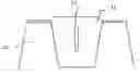
In the process for semiconductor devices getting more and more compact, shallow trench isolation (STI) is used to separate active areas 10 for forming respective elements. STI is formed between active areas 10 and is filled with dielectric 12, which can be oxide such as silicon oxide. However, a void 13 is likely to be generated in the step of filling with the dielectric 12, as shown in FIG. 1.
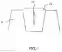
In DRAM process, such a condition also happens. With reference to FIG. 2, which is a schematic top view of a gate region structure of a DRAM, reference number 20 indicates an active area, 21 indicates a gate line, 24 indicates a deep trench. As shown in the drawing, the adjacent portion between the active areas is short. Reference number 23 indicates a void formed in the dielectric filled in the STI between the active areas 20. The existence of the void 23 may influence the electric performance of the semiconductor structure. However, such a void is very small and is hardly found during the process. Usually, the existence of the void only can be found in the electric testing, which is performed after the wafer is finished, cut into chips and packed. Accordingly, a waste of process is generated.
Therefore, there is a need for a solution to overcome the problems stated above. The present invention satisfies such a need.
SUMMARY OF THE INVENTIONAn objective of the present invention is to provide a STI void detecting method for semiconductor wafers. The method of the present invention can find in time whether there is any void formed in STI, so that the defective products can be found in the early stage, thereby reducing the waste of the cost and working hours.
Another objective of the present invention is to provide a STI void detecting region structure for semiconductor wafers. By forming and testing the testing region structure of the present invention, whether there is any void formed in STI can be found in time.
According to an aspect of the present invention, a shallow trench isolation void detecting method for a semiconductor wafer comprises steps of assigning a testing region in a predetermined region of the semiconductor wafer; forming active areas and gate lines inter with the active areas in said detecting region by a synchronous process for other regions, filling a trench between the active areas with dielectric, the adjacent portion between the active areas having at least a predetermined length; and detecting the electric values of the gate lines to determine whether there is a void formed in the dielectric filled in the trench between the active areas.
According to another aspect of the present invention, a testing region structure for semiconductor wafer STI void detecting is formed on the wafer by a process synchronizing for other portions of the wafer. The testing region structure comprises a plurality of active areas, trenches between the active areas being filled with dielectric, and the portions of the active areas adjacent to each other having at least a predetermined length; and a plurality of gate lines inter with the active areas.
BRIEF DESCRIPTION OF THE DRAWINGSThe following drawings are only for illustrating the mutual relationships between the respective portions and are not drawn according to practical dimensions and ratios. In addition, the like reference numbers indicate the similar elements.
FIG. 1 shows a schematic sectional diagram illustrating a void formed in a STI of a semiconductor device;
FIG. 2 is a schematic top view showing the arrangement of the active areas and gate lines of a semiconductor device in prior art; and
FIG. 3 is a schematic top view showing the arrangement of the active areas and gate lines of a semiconductor device in accordance with an embodiment of the present invention.
DETIALED DESCRIPTION OF THE PREFERRED EMBODIMENTAn embodiment of the present invention will be described in detail with reference to the accompanying drawings.
According to an embodiment of the present invention, at predetermined locations on the wafer, preferably the cut lines portion, testing regions comprising active areas and gate lines are produced by the synchronous process for other portions of the wafer.
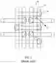
As shown in FIG. 3, the sections of active areas 30 in the testing region are formed as long strips. Accordingly, the active areas 30 are adjacent to each other. Shallow trenches formed between the active areas 30 are filled with dielectric 32 by the process synchronous with other portions of the wafer. As shown, in the present embodiment, the active areas 30 are preferably formed as parallel strips. Since the length of the portions of two active areas 30 adjacent to each other is very long, if there is a void 33 formed in the dielectric 32, the void 33 will be a long void. Gate lines 31′ in the testing region are arranged at an interval the same as the gate lines in other non-testing regions. As shown, since the section of the void 33 is long, the void 33 crosses at least two gate lines 31′. Accordingly, for example, it is easy to detect whether there is a void existing by measuring the potentials of the gate lines 31′ in the testing region.
According to the present embodiment, for the sake of convenience of measuring, the gate 31 can be formed as a comb-shaped gate. That is, the odd gate lines connected together, while the even gate lines connected together, thereby forming a dual-comb structure. Then the potential of a plurality of gate lines can be measured at a time.
The testing region is produced synchronously with other regions of the wafer. Accordingly, if a void is detected in the testing region, it can be determined that there are voids formed in other portions of the wafer. Then the detective products can be found and eliminated at an early stage, but not the stage after the wafer is cut into chips and packed. Thus, unnecessary working process is avoided, and therefore the working hours and cost are reduced.
While the embodiment of the present invention is illustrated and described, various modifications and alterations can be made by persons skilled in this art. The embodiment of the present invention is therefore described in an illustrative but not restrictive sense. It is intended that the present invention may not be limited to the particular forms as illustrated, and that all modifications and alterations which maintain the spirit and realm of the present invention are within the scope as defined in the appended claims.
Claims
1. A method for detecting STI void of semiconductor wafer, comprising steps of
assigning a test region in a predetermined region of the wafer;
forming active areas, trenches between the active areas and gate lines intersecting with tthe active areas, said trenches being filled with dielectric, and said active areas having their adjacent portion reaching at least a predetermined length; and
measuring the electric values of said gate lines to determine whether there is a void formed in the trench.
2. The method as claimed in claim 1, wherein said active areas in the testing region are formed as parallel strips.
3. The method as claimed in claim 1, wherein odd ones of said gate lines are connected together, while even ones of the gate lines are connected together, so as to form a dual-comb structure.
4. The method as claimed in claim 3, wherein said measuring step is to measure the potentials of the comb structure of the odd gate lines and the comb structure of the even gate lines.
5. The method as claimed in claim 1, wherein the testing region is formed on a predetermined cutting line of the wafer.
6. A testing region structure for STI void detection of semiconductor wafer, said test region structure being formed on the wafer by a process synchronous with other portions of the wafer, said structure comprising:
a plurality of active areas, the adjacent portion between two active areas reaching at least a predetermined length;
a plurality of trenches formed between the active areas and being filled with dielectric; and
a plurality of gate lines intersecting with said active areas.
7. The structure as claimed in claim 6, wherein said active areas in the testing region are formed as parallel strips.
8. The structure as claimed in claim 6, wherein the odd ones of the gate lines are connected together, while the even ones of the gate lines are connected together, so as to constitute a dual-comb structure.
9. The structure as claimed in claim 6, wherein the testing region structure is formed on a predetermined cutting line of the wafer.
Images & Drawings included:
Sources:
- United States Patent and Trademark Office - verify current appl. status at the USPTO↗
Similar patent applications:
Recent applications in this class:
- » 20250293101 2025-09-18
CONTAMINATION DETECTION METHOD - » 20250293100 2025-09-18
MANUFACTURING METHOD FOR SEMICONDUCTOR DEVICE AND SEMICONDUCTOR WAFERS - » 20250293099 2025-09-18
SAME-SIDE COMBINED ELECTRICAL/OPTICAL TESTING AT MULTIPLE IC DEVICE FABRICATION STAGES - » 20250285923 2025-09-11
SEMICONDUCTOR DEVICE INCLUDING A TEST LINE PORTION AND METHOD OF MAKING AND TESTING THE SAME - » 20250266304 2025-08-21
Semiconductor Wafer with Process Control Monitor Structures - » 20250266303 2025-08-21
DEVICE PACKAGE AND MANUFACTURING METHOD THEREOF - » 20250253194 2025-08-07
IN-SITU THROUGH SILICON VIA CHARACTERIZATION AND MONITORING IN SEMICONDUCTOR DEVICES - » 20250233029 2025-07-17
SEMICONDUCTOR DEVICE AND TEST METHOD OF THE SAME - » 20250226270 2025-07-10
SEMICONDUCTOR STRUCTURE - » 20250218877 2025-07-03
Semiconductor Structure and Method of Manufacture
Recent applications for this Assignee:
- » 20190109113 2019-04-11
Semiconductor apparatus and method for preparing the same - » 20190081018 2019-03-14
Method for preparing a semiconductor package - » 20180374818 2018-12-27
Method for preparing a semiconductor apparatus - » 20180233486 2018-08-16
Die device, semiconductor device and method for making the same - » 20180226332 2018-08-09
Package structure and manufacturing method thereof - » 20180197284 2018-07-12
Method of recognizing wafer - » 20180196769 2018-07-12
Comparative forwarding circuit providing first datum and second datum to one of first circuit and second circuit according to target address - » 20180190607 2018-07-05
Semiconductor package and method for preparing the same - » 20180182588 2018-06-28
System and method for blowing a fuse - » 20180138145 2018-05-17
Semiconductor package and manufacturing method thereof