Method of manufacturing NAND flash device
US20050106814A1
2005-05-19
10/887,964
2004-07-09
✅ Patent granted
US 6,979,618 B2
2005-12-27
-
-
William M. Brewster
2024-07-09
Abstract:
The present invention discloses a method of manufacturing a NAND flash device which can improve uniformity of disturb fail characteristics by performing an annealing process after an ion implantation process for forming a P well, reduce a fail bit count by performing an annealing process after an ion implantation process for controlling a threshold voltage and before a process for forming a high voltage gate oxide film, and prevent disturb fail by omitting an STI ion implantation process in a cell region.
Assignee:
- Hynix Semiconductor Inc. 235 🇰🇷 Kyungki-do, South Korea
Interested in similar patents?
Get notified when new applications in this technology area are published.
Classification:
H01L29/40114 » CPC main
Semiconductor devices adapted for rectifying, amplifying, oscillating or switching, or capacitors or resistors with at least one potential-jump barrier or surface barrier, e.g. PN junction depletion layer or carrier concentration layer; Details of semiconductor bodies or of electrodes thereof; Multistep manufacturing processes therefor; Electrodes ; Multistep manufacturing processes therefor; Multistep manufacturing processes for data storage electrodes the electrodes comprising a conductor-insulator-conductor-insulator-semiconductor structure
H01L21/324 » CPC further
Processes or apparatus adapted for the manufacture or treatment of semiconductor or solid state devices or of parts thereof; Manufacture or treatment of semiconductor devices or of parts thereof the devices having at least one potential-jump barrier or surface barrier, e.g. PN junction, depletion layer or carrier concentration layer the devices having semiconductor bodies comprising elements of Group IV of the Periodic System or AB compounds with or without impurities, e.g. doping materials; Treatment of semiconductor bodies using processes or apparatus not provided for in groups - Thermal treatment for modifying the properties of semiconductor bodies, e.g. annealing, sintering
Description
BACKGROUND1. Field of the Invention
The present invention relates to a method of manufacturing a NAND flash device, and more particularly to, a method of manufacturing a NAND flash device which can prevent program disturb defects from being generated due to damages of ion implantation processes for controlling wells and a threshold voltage.
2. Discussion of Related Art
An ion implantation process for forming a triple well, an ion implantation process for forming a P well, an ion implantation process for forming an N well, an ion implantation process for controlling a threshold voltage, a process for forming a gate oxide film for a high voltage device in a high voltage device region, a process for forming a tunnel oxide film in a cell region, and a process for forming an element isolation film are sequentially performed before a process for forming a gate of 0.115 μm tech of NAND flash EEPROM. Gate electrodes, namely a floating gate electrode and a control gate electrode are formed on the resulting structure.
However, an annealing process is not at all performed after the ion implantation processes for controlling the wells and the threshold voltage, so that damages of a semiconductor substrate by the ion implantation cannot be cured. Such damages cause dislocation of the semiconductor substrate and generate leakage current paths on the semiconductor substrate, which results in program disturb fail.
SUMMARY OF THE INVENTIONThe present invention is directed to a method of manufacturing a NAND flash device which can prevent program disturb fail by performing a P well annealing process after an ion implantation process for forming a P well, and performing an annealing process before a process for forming a gate oxide film for a high voltage device.
One aspect of the present invention is to provide a method of manufacturing a NAND flash device, including the steps of: performing a first ion implantation process for forming a triple well and a second ion implantation process for forming a P well on a semiconductor substrate; performing a first annealing process for curing damages of the semiconductor substrate by the first and second ion implantation processes; performing a third ion implantation process for forming an N well and a fourth ion implantation process for controlling a threshold voltage; forming a high voltage gate oxide film in a high voltage device region, and forming a tunnel oxide film in a low voltage device region and a cell region; and sequentially forming an element isolation film and a gate electrode.
Preferably, the method of manufacturing the NAND flash device further includes a step for performing a second annealing process for curing damages of the semiconductor substrate by the third and fourth ion implantation processes after the fourth ion implantation process and before the process for forming the high voltage gate oxide film.
Preferably, the first and second annealing processes are performed at a temperature ranging from 700 to 1100° C. under N2 gas atmosphere.
According to another aspect of the present invention, a method of manufacturing a NAND flash device includes the steps of: forming a triple well, a P well, an N well and an ion layer for controlling a threshold voltage on a semiconductor substrate by performing predetermined ion implantation processes; performing an annealing process for curing damages of the semiconductor substrate by the ion implantation processes; forming a high voltage gate oxide film in a high voltage device region, and forming a tunnel oxide film in a low voltage device region and a cell region; and sequentially forming an element isolation film and a gate electrode.
Preferably, the annealing process is performed at a temperature ranging from 700 to 1100° C. under N2 gas atmosphere.
BRIEF DESCRIPTION OF THE DRAWINGSFIG. 1 is a concept diagram showing disturb defects of a flash device;
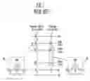
FIGS. 2A and 2B are cross-sectional diagrams illustrating sequential steps of a method of manufacturing a NAND flash device in accordance with the present invention;
FIG. 3A is a graph showing a bypass disturb fail bit count by an annealing process after a process for forming a P well;
FIG. 3B is a graph showing a program disturb fail bit count;
FIG. 4 is a graph showing a bypass disturb fail bit count by an STI ion implantation process; and
FIG. 5 is a graph showing a program disturb fail bit count by an annealing process before a process for forming a high voltage gate oxide film.
DETAILED DESCRIPTION OF PREFERRED EMBODIMENTSA method of manufacturing a NAND flash device in accordance with a preferred embodiment of the present invention will now be described in detail with reference to the accompanying drawings. Wherever possible, the same reference numerals will be used throughout the drawings and the description to refer to the same or like parts.
FIG. 1 is a concept diagram showing disturb defects of a flash device.
Referring to FIG. 1, the disturb in a NAND flash EEPROM is divided into two modes, bypass disturb Vpass 10 and program disturb Vpgm 20. The bypass disturb fail occurs when an intrinsic program speed (F-N tunneling) is abnormally high for normal cells. That is, the bypass disturb fail is generated in cells receiving a bypass voltage. The program disturb fail occurs when channel boosting is not normally performed due to a leakage current generated between an inversion layer and a lower semiconductor substrate by dislocation of the substrate. That is, the program disturb fail is generated in cells (program cells) receiving a program voltage. In accordance with the present invention, an annealing process can prevent disturb defects of the flash device.
FIGS. 2A and 2B are cross-sectional diagrams illustrating sequential steps of the method of manufacturing the NAND flash device in accordance with the present invention.
As illustrated in FIG. 2A, an ion implantation process for forming a triple well is performed on a semiconductor substrate 110, to form a triple well 120. An ion implantation process for forming a P well is performed in a PMOS device formation region, to form a P well 130. A first annealing process is performed to compensate for damages of the semiconductor substrate 110 by the ion implantation processes, activate ions and improve disturb uniformity.
Preferably, the first annealing process is performed at a temperature ranging from 700 to 1100° C. under N2 gas atmosphere for about 20 to 40 min. A high temperature thermal oxidation process for forming a screen oxide film used as a buffer film in a succeeding ion implantation process can be performed with the first annealing process.
As shown in FIG. 2B, an ion implantation process for forming an N well is performed to form an N well 140. An ion implantation process for controlling a threshold voltage is performed to form an ion layer (not shown) for controlling a threshold voltage. A second annealing process is performed to compensate for damages of the semiconductor substrate 10 by the ion implantation processes, thereby remarkably reducing a fail bit count.
Preferably, the second annealing process is performed at a temperature ranging from 700 to 1100° C. under N2 gas atmosphere for about 1 to 100 min. The second annealing process is selected from an annealing process using a furnace and a rapid thermal process (RTP).
In order to form the wells and the ion layer for controlling the threshold voltage, ion implantation processes can be performed merely in target regions on the semiconductor substrate 110 according to a patterning process using a photoresist film. In addition, doses and Rp of the ion implantation processes can be varied under the conditions of the devices formed in the upper sides.
A gate oxide film (not shown) for a high voltage device is formed over the resulting structure where the wells and the ion layer for controlling the threshold voltage have been formed, and removed in low voltage device and cell formation regions. A tunnel oxide film (not shown) is formed on the resulting structure. An element isolation film (not shown) is formed according to a self aligned shallow trench isolation (SA-STI) process. A polysilicon film (not shown) for a floating gate and a pad insulation film (not shown) are formed on the tunnel oxide film. An element isolation trench (not shown) is formed by etching the pad insulation film, the polysilicon film, the tunnel oxide film (gate oxide film) and the semiconductor substrate 110. An element isolation film is formed by filling the element isolation trench with an oxide film, and performing a planarization process using the pad insulation film as a barrier film. Generally, in order to remove sub threshold hump characteristics of a low voltage NMOS transistor, an STI ion implantation process is performed to compensate for boron segregation on the STI sidewalls after the process for etching the trench. However, in accordance with the present invention, the STI ion implantation process is not performed in the cell region, thereby reducing the fail bit count by three to four times. For this, a photoresist film pattern is formed on the cell region, the STI ion implantation process is performed thereon, the photoresist film is removed and the oxide film is filled and planarized, after the process for forming the element isolation trench.
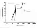
FIG. 3A is a graph showing a bypass disturb fail bit count by the annealing process after the process for forming the P well, and FIG. 3B is a graph showing a program disturb fail bit count.
As depicted in FIGS. 3A and 3B, when the disturb of the flash device is measured after forming the P well and performing the annealing process thereon at about 950° C. for about 30 min., uniformity of the bypass disturb and program disturb characteristics is improved. That is, damages of the semiconductor substrate by the high energy well ion implantation process are cured by the annealing process. As shown in FIG. 3A, on the basis of cumulative probability distribution, the fail bit count is distributed from 100 to 100000ea without the annealing process, but aligned in about 100ea after the annealing process. As illustrated in FIG. 3B, the fail bit count is distributed from 100 to 10000ea without the annealing process, but aligned in about 200ea after the annealing process.
FIG. 4 is a graph showing a bypass disturb fail bit count by the STI ion implantation process.
Referring to FIG. 4, the STI ion implantation process is performed on the sidewalls of the trench to compensate for boron variations inside the semiconductor substrate due to the etching process for forming the trench during the STI process for forming the element isolation film, which increases the bypass disturb fail bit count of the cell. That is, when the cumulative probability is 40%, the fail bit count is about 1000ea after the ion implantation process, but about 300ea without the ion implantation process. In the case that the STI ion implantation process is applied to the cell region, the bypass fail bit count is increased by three to four times. Accordingly, when the STI ion implantation process is not performed in the cell region, the fail bit count can be considerably reduced.
FIG. 5 is a graph showing a program disturb fail bit count by the annealing process before the process for forming the high voltage gate oxide film.
As shown in FIG. 5, the program disturb characteristics are remarkably improved by performing the annealing process before the process for forming the high voltage gate oxide film, namely after the process for forming the N well and the ion layer for controlling the threshold voltage. When the cumulative probability is 50%, the fail bit count is varied by six to seven times according to the annealing process. That is, the thermal annealing process can cure defects of the semiconductor substrate after the ion implantation process for controlling the threshold voltage.
As a result, uniformity of the disturb fail characteristics can be improved by additionally performing the annealing process after the process for forming the P well, and the fail bit count can be reduced by performing the annealing process after the ion implantation process for controlling the threshold voltage and before the process for forming the high voltage gate oxide film. It implies that the annealing process can cure the defects of the semiconductor substrate resulting from the ion implantation damages. Moreover, the STI ion implantation process is not applied to the cell region, to prevent the disturb fail.
As described above, in accordance with the present invention, uniformity of the disturb fail characteristics of the flash device can be improved by performing the annealing process after the ion implantation process for forming the P well.
In addition, the fail bit count can be reduced by performing the annealing process after the ion implantation process for controlling the threshold voltage and before the process for forming the high voltage gate oxide film.
Furthermore, the STI ion implantation process is not performed in the cell region, thereby preventing the disturb fail.
Although the present invention has been described in connection with the embodiment of the present invention illustrated in the accompanying drawings, it is not limited thereto. It will be apparent to those skilled in the art that various substitutions, modifications and changes may be made thereto without departing from the scope and spirit of the invention.
Claims
1. A method of manufacturing a NAND flash device, comprising the steps of:
performing a first ion implantation process for forming a triple well and a second ion implantation process for forming a P well on a semiconductor substrate;
performing a first annealing process for curing damages of the semiconductor substrate by the first and second ion implantation processes;
performing a third ion implantation process for forming an N well and a fourth ion implantation process for controlling a threshold voltage;
forming a high voltage gate oxide film in a high voltage device region, and forming a tunnel oxide film in a low voltage device region and a cell region; and
sequentially forming an element isolation film and a gate electrode.
2. The method of claim 1, further comprising a step for performing a second annealing process for curing damages of the semiconductor substrate by the third and fourth ion implantation processes after the fourth ion implantation process and before the process for forming the high voltage gate oxide film.
3. The method of claim 1, wherein the first and second annealing processes are performed at a temperature ranging from 700 to 1100° C. under N2 gas atmosphere.
4. The method of claim 2, wherein the first and second annealing processes are performed at a temperature ranging from 700 to 1100° C. under N2 gas atmosphere.
5. A method of manufacturing a NAND flash device, comprising the steps of:
forming a triple well, a P well, an N well and an ion layer for controlling a threshold voltage on a semiconductor substrate by performing predetermined ion implantation processes;
performing an annealing process for curing damages of the semiconductor substrate by the ion implantation processes;
forming a high voltage gate oxide film in a high voltage device region, and forming a tunnel oxide film in a low voltage device region and a cell region; and
sequentially forming an element isolation film and a gate electrode.
6. The method of claim 5, wherein the annealing process is performed at a temperature ranging from 700 to 1100° C. under N2 gas atmosphere.
Images & Drawings included:


Sources:
- United States Patent and Trademark Office - verify current appl. status at the USPTO↗
Similar patent applications:
- » 20050124103
Method for manufacturing NAND flash device - » 20050272204
Method for manufacturing NAND flash device - » 20050208721
Method for manufacturing NAND flash device - » 20080003744
METHOD OF MANUFACTURING NAND FLASH MEMORY DEVICE - » 20070122972
Method of manufacturing NAND flash memory device - » 20080003743
Method of manufacturing NAND flash memory device - » 20070117318
Method of manufacturing NAND flash memory device - » 20070087538
Method of manufacturing NAND flash memory device - » 20070155098
Method of manufacturing NAND flash memory device - » 20130102151
Methods of manufacturing NAND flash memory devices
Recent applications in this class:
- » 20250056863 2025-02-13
SEMICONDUCTOR DEVICE WITH NON-VOLATILE MEMORY CELL AND MANUFACTURING METHOD THEREOF - » 20240304681 2024-09-12
SEMICONDUCTOR DEVICE AND METHOD OF FORMING THE SAME - » 20240297226 2024-09-05
SEMICONDUCTOR STRUCTURE - » 20240072129 2024-02-29
STRUCTURE OF FLASH MEMORY CELL - » 20230411462 2023-12-21
Profile shaping for control gate recesses - » 20230378284 2023-11-23
Semiconductor device with non-volatile memory cell and manufacturing method thereof - » 20230335602 2023-10-19
Semiconductor structure and method of forming the same - » 20230170392 2023-06-01
METHOD FOR MANUFACTURING GATE OF NAND FLASH - » 20230112478 2023-04-13
Memory Device Having Nano-Structure and Method for Fabricating the Same - » 20220359674 2022-11-10
Semiconductor device with non-volatile memory cell and manufacturing method thereof
Recent applications for this Assignee:
- » 20110248324 2011-10-13
DUAL-GATE NON-VOLATILE FERROELECTRIC MEMORY - » 20110114736 2011-05-19
INTEGRATED CIRCUIT WITH EMBEDDED RFID - » 20090010082 2009-01-08
Data transfer apparatus in semiconductor memory device and method of controlling the same - » 20080176047 2008-07-24
Liquid Composition for Immersion Lithography and Lithography Method Using the Same - » 20080019204 2008-01-24
Apparatus and Method for Supplying Power in Semiconductor Device - » 20070298523 2007-12-27
Silicon wafers and method of fabricating the same - » 20070187620 2007-08-16
Apparatus and method for partial ion implantation - » 20070176218 2007-08-02
Dual-gate non-volatile ferroelectric memory - » 20070163625 2007-07-19
Method for forming a photoresist pattern - » 20070141837 2007-06-21
Contact structure of semiconductor device and method for fabricating the same