Apparatus for separating cull of semiconductor package molding system
US20050125996A1
2005-06-16
10/875,477
2004-06-24
✅ Patent granted
US 7,299,544 B2
2007-11-27
-
-
Minh Trinh
2025-08-10
Abstract:
Disclosed is an apparatus for separating culls coupled to a lead frame when a semiconductor chip is molded. The apparatus includes a lower plate, on which culls coupled to a lead frame are placed, an upper plate pressing culls placed on the lower plate in order to separate culls from the lead frame, a pilot pin installed in the upper plate by passing through the upper plate in order to press culls together with the upper plate when the upper plate presses the culls, and a sensor unit installed adjacent to the movement path of the pilot pin so as to detect a movement of the pilot pin. When culls are separated, faults of articles caused by a molding material insufficiently filled in a mold are checked through detecting a movement of the pilot pin.
Assignee:
- HYNIX SEMICONDUCTOR INC. 1,335 🇰🇷 Kyoungki-do, South Korea
Interested in similar patents?
Get notified when new applications in this technology area are published.
Classification:
H01L21/4842 » CPC main
Processes or apparatus adapted for the manufacture or treatment of semiconductor or solid state devices or of parts thereof; Manufacture or treatment of semiconductor devices or of parts thereof the devices having at least one potential-jump barrier or surface barrier, e.g. PN junction, depletion layer or carrier concentration layer; Manufacture or treatment of parts, e.g. containers, prior to assembly of the devices, using processes not provided for in a single one of the subgroups -; Conductive parts; Flat leads, e.g. lead frames with or without insulating supports Mechanical treatment, e.g. punching, cutting, deforming, cold welding
B29C45/38 » CPC further
Injection moulding, i.e. forcing the required volume of moulding material through a nozzle into a closed mould; Apparatus therefor; Component parts, details or accessories; Auxiliary operations Cutting-off equipment for sprues or ingates
B29C45/14655 » CPC further
Injection moulding, i.e. forcing the required volume of moulding material through a nozzle into a closed mould; Apparatus therefor incorporating preformed parts or layers, e.g. injection moulding around inserts or for coating articles for obtaining an insulating effect, e.g. for electrical components connected to or mounted on a carrier, e.g. lead frame
Y10T29/49121 » CPC further
Metal working; Method of mechanical manufacture; Electrical device making; Conductor or circuit manufacturing Beam lead frame or beam lead device
Y10T29/49146 » CPC further
Metal working; Method of mechanical manufacture; Electrical device making; Conductor or circuit manufacturing; On flat or curved insulated base, e.g., printed circuit, etc.; Assembling to base an electrical component, e.g., capacitor, etc. with encapsulating, e.g., potting, etc.
Y10T29/49821 » CPC further
Metal working; Method of mechanical manufacture; Disassembling by altering or destroying work part or connector
Y10T29/53052 » CPC further
Metal working; Means to assemble or disassemble with control means energized in response to activator stimulated by condition sensor; Multiple station assembly or disassembly apparatus including position sensor
Y10T29/5307 » CPC further
Metal working; Means to assemble or disassemble with control means energized in response to activator stimulated by condition sensor; Responsive to work or work-related machine element with means to fasten by deformation Self-piercing work part
Y10T29/53087 » CPC further
Metal working; Means to assemble or disassemble with signal, scale, illuminator, or optical viewer
Y10T29/53274 » CPC further
Metal working; Means to assemble or disassemble Means to disassemble electrical device
B23P19/00 IPC
Machines for simply fitting together or separating metal parts or objects, or metal and non-metal parts, whether or not involving some deformation ; Tools or devices therefor so far as not provided for in other classes
Description
BACKGROUND OF THE INVENTION1. Field of the Invention
The present invention relates to a cull separation apparatus of a semiconductor package molding system, and more particularly to an apparatus separating culls coupled to a lead frame when a semiconductor chip is molded.
2. Description of the Prior Art
In order to fabricate a semiconductor package, a molding process is carried out in order to surround a semiconductor chip with mold material, such as thermosetting resin (for example, epoxy resin), after performing a bonding wire process for protecting the semiconductor chip from external impact or external environment. That is, since the semiconductor chip is surrounded by mold material through the molding process, the semiconductor chip may be prevented from being damaged by an external contamination source or external impact.
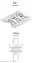
By-products called “culls” are created when performing such a molding process. That is, as shown in FIG. 1, culls 3 are coupled to a lead frame 2 having semiconductor chips 1 as by-products. This is because a mold for performing the molding process has a structure, which forms culls.
Accordingly, as shown in FIG. 2, it is necessary to separate the culls 3 from the lead frame 2 by using a cull separation apparatus. Firstly, the culls 3 coupled with the lead frame 2 are placed on a lower plate 21. Then, the culls 3 are pressed by means of an upper plate 22. At this time, pressing action for the upper plate 22 is carried out through up and down movements of a cylinder connected to the upper plate 22. Accordingly, the culls 3 are broken due to the pressing action of the upper plate 22, so that the culls 3 are separated from the lead frame 2.
When such a molding process is performed, the molding material is often insufficiently filled in the mold, thereby generating faults. However, it is not easy to detect such faults in an early stage. That is, after the molding process has been finished, a separate inspection process utilizing X-rays must be carried out in order to detect the faults of articles.
Accordingly, since the faults of articles cannot be detected in the early stage during the molding process, productivity of semiconductor devices is decreased.
SUMMARY OF THE INVENTIONTherefore, the present invention has been made to solve the above-mentioned problems occurring in the prior art, and an object of the present invention is to provide a cull separation apparatus of a semiconductor package molding system capable of detecting faults in an early stage of the faults, which may be generated due to molding material insufficiently filled in a mold when a semiconductor package molding process is carried out.
In order to accomplish this object, there is provided a cull separation apparatus of a semiconductor package molding system, the cull separation apparatus comprising a lower plate, on which culls coupled to a lead frame are placed; an upper plate pressing culls placed on the lower plate in order to separate culls from the lead frame; a pilot pin installed in the upper plate by passing through the upper plate in order to press culls together with the upper plate when the upper plate presses the culls; and a sensor unit installed adjacent to the movement path of the pilot pin so as to detect a movement of the pilot pin.
The sensor unit is installed on an upper surface of the upper plate and includes a light receiving device and a light emitting device.
According to the preferred embodiment of the present invention, a chuck separation device including a pilot pin and a sensor unit is further provided. Therefore, when culls are separated, faults of articles caused by the molding material insufficiently filled in a mold can be instantly checked through detecting the movement of the pilot pin. Accordingly, it is not necessary to separately carry out a checking process for faults caused by the molding material insufficiently filled in the mold.
BRIEF DESCRIPTION OF THE DRAWINGSThe above object, features and advantages of the present invention will be more apparent from the following detailed description taken in conjunction with the accompanying drawings, in which:
FIG. 1 is a view showing a molded semiconductor package;
FIG. 2 is a schematic sectional view showing a cull separation apparatus of a conventional semiconductor package molding system; and
FIGS. 3A and 3B are views showing operational states of a cull separation apparatus of a semiconductor package molding system according to one embodiment of the present invention.
DETAILED DESCRIPTION OF THE PREFERRED EMBODIMENTSHereinafter, a preferred embodiment of the present invention will be described with reference to the accompanying drawings. In the following description and drawings, the same reference numerals are used to designate the same or similar components, and so repetition of the description on the same or similar components will be omitted.
FIGS. 3A and 3B are views showing operational states of a cull separation apparatus of a semiconductor package molding system according to one embodiment of the present invention.
Referring to FIG. 3A, the cull separation apparatus includes an upper plate 32 and a lower plate 30. Herein, culls 31 coupled to a lead frame are placed on the lower plate 30, and the upper plate 32 presses the culls 31 placed on the lower plate 30. At this time, the upper plate 32 is connected to a cylinder (not shown) in order to press the culls 31. Accordingly, the culls 31 are pressed by the upper plate 32 in a state in which the culls 31 are placed on the lower plate 30, so the culls 31 are broken by the pressing action of the upper plate 32 and are separated from the lead frame.
In addition, a pilot pin 33 is provided in the upper plate 32 by passing through the upper plate 32. Herein, the pilot pin 33 presses the culls 31 together with the upper plate 32 when the upper plate 21 presses the culls 31. To this end, the pilot pin 33 includes a stopper and a spring. Also, a sensor unit 34, such as a light receiving device and a light emitting device, is installed adjacent to an inlet of the upper plate 32, in which the inlet of the upper plate 32 may provide a movement path for the pilot pin 33 installed in the upper plate 32. Accordingly, the sensor unit 34 can detect a movement of the pilot pin 34.
As shown in FIG. 3A, by providing the pilot pin 33 and the sensor unit 34, the pilot pin 33 also presses the culls 31 when the upper plate 32 presses the culls 31. The pilot pin 33 moves along with the upper plate 32 so as to separate the culls from the lead frame. At this time, if the culls 31 are formed in a state in which molding material is sufficiently filled in the mold, the pilot pin 33 is scarcely moved. Thus, the sensor unit 34 does not operate.
However, as shown in FIG. 3B, if culls 31 are formed in a state in which molding material is insufficiently filled in the mold, the pilot pin 33 breaks the culls 31 by pressing the culls 31 when the culls 31 are separated from the lead frame by means of the upper plate 32. Accordingly, the pilot pin 33 moves towards the lower plate. At this time, the sensor unit 34 may operate so as to perform a sensing operation and to display a sensing result.
Accordingly, a fault caused by molding material insufficiently filled in the mold can be instantly detected when the culls 31 are separated from the lead frame. When the molding material is insufficiently filled in the mold, the culls 31 are generally formed with a thin thickness. For this reason, the culls 31 are easily broken when the pilot pin 33 presses the culls 31, so faults of the culls 31 can be easily checked.
As described above, according to the present invention, culls having a fault can be instantly checked when the culls are separated from the lead frame. In addition, the fault of the culls can be checked without using a separate apparatus. Thus, the present invention can improve productivity of semiconductor devices.
Although a preferred embodiment of the present invention has been described for illustrative purposes, those skilled in the art will appreciate that various modifications, additions and substitutions are possible, without departing from the scope and spirit of the invention as disclosed in the accompanying claims.
Claims
1. An apparatus for separating a cull of a molding system of a semiconductor package, the apparatus comprising:
a lower plate, on which culls coupled to a lead frame are placed;
an upper plate pressing culls placed on the lower plate in order to separate culls from the lead frame;
a pilot pin installed in the upper plate by passing through the upper plate in order to press culls together with the upper plate when the upper plate presses the culls; and
a sensor unit installed adjacent to the movement path of the pilot pin so as to detect a movement of the pilot pin.
2. The apparatus as claimed in claim 1, wherein the sensor unit is installed on an upper surface of the upper plate and includes a light receiving device and a light emitting device.
Images & Drawings included:


Sources:
- United States Patent and Trademark Office - verify current appl. status at the USPTO↗
Recent applications in this class:
- » 20250273478 2025-08-28
INFRARED LASER DEBOND PROCESS FOR FUSION-BONDED OR HYBRID-BONDED DIE COMPLEXES ON REUSABLE CARRIER WAFERS - » 20250038009 2025-01-30
STRESS RELIEF SAWN QUAD FLAT NO-LEAD SEMICONDUCTOR PACKAGE - » 20250006508 2025-01-02
METHOD OF MANUFACTURING LEAD FRAME - » 20240355639 2024-10-24
PACKAGE STRUCTURE AND METHOD OF MANUFACTURING THE SAME - » 20240258120 2024-08-01
LASER-CUT LEAD FRAME FOR INTEGRATED CIRCUIT (IC) PACKAGES - » 20240249955 2024-07-25
METHOD OF MANUFACTURING MULTI-DIE SEMICONDUCTOR DEVICES AND CORRESPONDING MULTI-DIE SEMICONDUCTOR DEVICE - » 20240222139 2024-07-04
MICROELECTRONIC PACKAGE STRUCTURES WITH SOLDER JOINT ASSEMBLIES HAVING ROUGHENED BUMP STRUCTURES - » 20240194494 2024-06-13
INTERCONNECT SINGULATION - » 20240021436 2024-01-18
METHOD AND APPARATUS FOR MANUFACTURING A TERMINAL APPARATUS FOR CONNECTING AT LEAST ONE ELECTRICAL OR ELECTRONIC COMPONENT FOR AN ELECTRICAL OR ELECTRONIC MODULE - » 20230121743 2023-04-20
Interconnect singulation
Recent applications for this Assignee:
- » 20130181761 2013-07-18
Trimming of operative parameters in electronic devices based on corrections mappings - » 20130087919 2013-04-11
LIGHTWEIGHT AND COMPACT THROUGH-SILICON VIA STACK PACKAGE WITH EXCELLENT ELECTRICAL CONNECTIONS AND METHOD FOR MANUFACTURING THE SAME - » 20130027076 2013-01-31
APPARATUS FOR DETECTING PATTERN ALIGNMENT ERROR - » 20120322216 2012-12-20
METHOD FOR REDUCING POLY-DEPLETION IN DUAL GATE CMOS FABRICATION PROCESS - » 20120231635 2012-09-13
Template derivative for forming ultra-low dielectric layer and method of forming ultra-low dielectric layer using the same - » 20120231634 2012-09-13
Template derivative for forming ultra-low dielectric layer and method of forming ultra-low dielectric layer using the same - » 20120217637 2012-08-30
Semiconductor package having substrate for high speed semiconductor package - » 20120205802 2012-08-16
PRINTED CIRCUIT BOARD AND FLIP CHIP PACKAGE USING THE SAME WITH IMPROVED BUMP JOINT RELIABILITY - » 20120115278 2012-05-10
STACKED SEMICONDUCTOR PACKAGE WITHOUT REDUCTION IN DATA STORAGE CAPACITY AND METHOD FOR MANUFACTURING THE SAME - » 20120088336 2012-04-12
SEMICONDUCTOR PACKAGE HAVING AN IMPROVED CONNECTION STRUCTURE AND METHOD FOR MANUFACTURING THE SAME