Light shield process for solid-state image sensors
US20050127370A1
2005-06-16
11/042,936
2005-01-25
✅ Patent granted
US 7,091,532 B2
2006-08-15
-
-
William M. Brewster
2025-02-19
Abstract:
An image sensor includes a substrate containing photosensitive areas; an insulator spanning the substrate; and a first and second layer of a multi-layer metalization structure wherein the first layer forms the light shield regions over portions of the photosensitive area as well as forming circuit interconnections and barrier regions to prevent spiking into the substrate or gates at contacts in the non-imaging area, and the second layer spanning the interconnections and barrier regions of the first layer only over the non-imaging area.
Assignee:
- Eastman Kodak Company 4,928 🇺🇸 Rochester, NY, United States
Interested in similar patents?
Get notified when new applications in this technology area are published.
Classification:
H01L27/14601 » CPC main
Devices consisting of a plurality of semiconductor or other solid-state components formed in or on a common substrate including semiconductor components sensitive to infra-red radiation, light, electromagnetic radiation of shorter wavelength or corpuscular radiation and specially adapted either for the conversion of the energy of such radiation into electrical energy or for the control of electrical energy by such radiation; Devices controlled by radiation; Imager structures Structural or functional details thereof
H01L27/14806 » CPC further
Devices consisting of a plurality of semiconductor or other solid-state components formed in or on a common substrate including semiconductor components sensitive to infra-red radiation, light, electromagnetic radiation of shorter wavelength or corpuscular radiation and specially adapted either for the conversion of the energy of such radiation into electrical energy or for the control of electrical energy by such radiation; Devices controlled by radiation; Imager structures; Charge coupled imagers Structural or functional details thereof
H01L21/76 IPC
Processes or apparatus adapted for the manufacture or treatment of semiconductor or solid state devices or of parts thereof; Manufacture or treatment of devices consisting of a plurality of solid state components formed in or on a common substrate or of parts thereof; Manufacture of integrated circuit devices or of parts thereof; Manufacture of specific parts of devices defined in group Making of isolation regions between components
Description
CROSS-REFERENCE TO RELATED APPLICATIONSThis is a divisional of application Ser. No. 10/641,724, filed Aug. 15, 2004, METHOD FOR FORMING LIGHT SHIELD PROCESS FOR SOLID-STATE IMAGE SENSOR WITH MULTI-METALLIZATION LAYER by Eric G. Stevens.
FIELD OF THE INVENTIONThe invention relates generally to the field of light shields used on solid-state image sensors and, more particularly, to such light shields formed by sequential and selective etching of a bi-metal structure that is also used to form the electrical interconnections on the device.
BACKGROUND OF THE INVENTIONCurrently, image sensors are made of photosensitive sites, or pixels, over a portion of which light shields are disposed. These light shields are used to prevent light from entering certain portions of the pixel where it is not desired, e.g., over the vertical shift registers of an interline CCD imager. These image sensors also contain electrical interconnects or bus lines around the periphery of the photosensitive sites for passing electrical signals to processing circuitry on the chip.
To improve the optical performance of the image sensor, it is desirable to make the light shield regions relatively thin, as is well known in the art. Conversely, to improve the electrical performance of the interconnects, it is desirable to make them relatively thick to improve their conductivity. Due to these competing requirements, the light-shield and interconnect regions are typically formed using separate and isolated layers. This adds to process complexity. Furthermore, the additional isolation layer(s) between the light-shield and interconnect region can result in degraded optical performance, in a similar way that having a thick light shield would.
Subsequently, a need exists for improving the performance of such image sensors with simplified manufacturing methods and materials.
SUMMARY OF THE INVENTIONThe present invention is directed to overcoming one or more of the problems set forth above. Briefly summarized, according to one aspect of the present invention, the invention resides in an image sensor having a substrate containing photosensitive areas; an insulator spanning the substrate; and a first and second layer of a multi-layer metalization structure wherein the first layer forms light shield regions over select portions of the photosensitive area as well as forming circuit interconnections and barrier regions to prevent spiking into the substrate or gates at contacts in the non-imaging area, and the second layer spanning the interconnections and barrier regions of the first layer only over the non-imaging area.
These and other aspects, objects, features and advantages of the present invention will be more clearly understood and appreciated from a review of the following detailed description of the preferred embodiments and appended claims, and by reference to the accompanying drawings.
Advantageous Effect Of The Invention
The present invention has the advantage of providing thin light shields that are formed by sequential and selective etching of a thick, bi-metal structure that is also used to form the electrical interconnections on a solid-state image sensor.
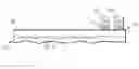
BRIEF DESCRIPTION OF THE DRAWINGSFIG. 1 is a side view in cross section of the image formed by the present invention;
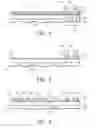
FIG. 2 is a side view in cross section of a subsequent step in forming the image sensor of FIG. 1;
FIG. 3 is a side view in cross section of a subsequent step of FIG. 2 in forming the image sensor of FIG. 1;
FIG. 4 is a side view in cross section of a subsequent step of FIG. 3 in forming the image sensor of FIG. 1; and
FIG. 5 is a side view in cross section of a subsequent step of FIG. 4 in forming the image sensor of FIG. 1.
DETAILED DESCRIPTION OF THE INVENTIONReferring to FIG. 1 of the preferred embodiment, there is shown an initial stage of forming an image sensor 10 of the present invention. This stage includes providing a substrate 20 having a plurality of photosensitive sites 30 that converts incident light into charge packets. An insulator 40 spans and covers the substrate, and a bi-metal structure 50 is disposed spanning and covering the insulator. Embedded within the insulator, may be other structure(s) such as gate electrodes, etc, which are not shown. The bi-metal structure 50 is preferably formed by two individual, adjacent and abutting layers where one layer is an alloy of titanium and tungsten 60 and the other layer is aluminum (or an alloy of aluminum and silicon) 70. Photoresist 80 is selectively disposed spanning and covering a portion of the layer of aluminum 70 that is in the non-imaging area 90. This non-imaging area 90 contains circuitry and other things such as the bus lines that will be used in operating the image sensor 10.
Referring to FIG. 2 of the preferred embodiment, there is shown the step of entirely etching the aluminum 70 over the photosensitive sites 30 with a chlorine-based etchant that etches the aluminum 70 but will not etch the tungsten and titanium alloy layer 60. The aluminum 70 over the non-imaging portion 90 is selectively etched in accordance with the patterned photoresist 80.
Referring to FIG. 3 of the preferred embodiment, there is shown photoresist 85 selectively patterned over portions of the titanium and tungsten alloy layer 60 spanning the photosensitive sites 30. Photoresist 85 is also patterned over the tungsten and titanium alloy layer 60 spanning the dark reference pixels or sites 100, and over the combination of titanium, tungsten 60 and aluminum 70 spanning the bus lines. Photoresist 85 may also be optionally patterned over the circuitry and bus lines in the non-imaging portion 90. Also note that in the preceding steps of patterning and etching the aluminum 70, that a portion of the aluminum layer 70 may be optionally left covering these dark reference pixels 100.
Referring to FIG. 4 of the preferred embodiment, there is shown the step of etching the tungsten and titanium alloy layer 60 in accordance with the patterned photoresist 85 with a fluorine-based etchant. This etchant etches the titanium and tungsten alloy layer 60, but does not etch the insulation layer 40 or any exposed and remaining portions of the aluminum layer 70.
Referring to FIG. 5 of the preferred embodiment, there is shown the step of stripping the photoresist 85 and continuing with the process. The remaining steps needed for completion of a commercially usable image sensor are well known in the art and will not be discussed in detail herein.
The invention has been described with reference to a preferred embodiment. However, it will be appreciated that variations and modifications can be effected by a person of ordinary skill in the art without departing from the scope of the invention. For example, use of other multi-layer metal structure materials and their corresponding selective etchants may be employed to create the invention.
Parts List
- 10 image sensor
- 20 substrate
- 30 photo sensitive sites
- 40 insulator
- 50 bi-metal structure
- 60 titanium and tungsten alloy
- 70 aluminum
- 80 photoresist
- 85 photoresist
- 90 non-imaging area
- 100 dark reference pixels
Claims
1. An image sensor comprising:
(a) a substrate having photosensitive areas;
(b) an insulator spanning the substrate; and
(c) a first and second layer of a multi-layer metalization structure wherein the first layer forms light shield regions over select portions of the photosensitive area as well as forming circuit interconnections and barrier regions to prevent spiking into the substrate or gates at contacts in the non-imaging area, and the second layer spanning the interconnections and barrier regions of the first layer only over the non-imaging area.
Images & Drawings included:

Sources:
- United States Patent and Trademark Office - verify current appl. status at the USPTO↗
Similar patent applications:
Recent applications in this class:
- » 20250072136 2025-02-27
Semiconductor Device, Solid-State Image Pickup Element, Imaging Device, and Electronic Apparatus - » 20240347554 2024-10-17
IMAGING ELEMENT AND IMAGING DEVICE - » 20240128282 2024-04-18
SEMICONDUCTOR DEVICE, ELECTRONIC DEVICE, AND METHOD OF CONTROLLING SEMICONDUCTOR DEVICE - » 20230187459 2023-06-15
INFRARED SENSOR AND METHOD OF MANUFACTURING INFRARED SENSOR - » 20230068256 2023-03-02
Image pickup device and electronic apparatus - » 20220415937 2022-12-29
IMAGING APPARATUS AND MANUFACTURING METHOD OF THE SAME - » 20220262830 2022-08-18
Radiation detector - » 20220181365 2022-06-09
Processing circuit and method for time-of-flight image sensor - » 20210257397 2021-08-19
Image pickup device and electronic apparatus - » 20210233946 2021-07-29
SEMICONDUCTOR DEVICE, SOLID-STATE IMAGE PICKUP ELEMENT, IMAGING DEVICE, AND ELECTRONIC APPARATUS
Recent applications for this Assignee:
- » 20250083435 2025-03-13
Inking system with plurality of fountain roller elements - » 20250083434 2025-03-13
INK TRAY INSERT - » 20240140743 2024-05-02
PRINTING PLATE PICKING SYSTEM AND PROCESS - » 20240118227 2024-04-11
MEDIA CONDUCTIVITY MEASUREMENT SYSTEM - » 20240053697 2024-02-15
Printer providing in-track error correction incorporating anti-aliasing at cross-track positions - » 20230314935 2023-10-05
Lithographic printing plate precursor and method of use - » 20230138562 2023-05-04
Electrophotographic printing system including lateral translations to reduce burn-in artifacts - » 20230137371 2023-05-04
Reproducing out-of-gamut spot colors on a color printer - » 20230133375 2023-05-04
User-preferred reproduction of out-of-gamut spot colors - » 20230130313 2023-04-27
Reducing artifacts using alternating light source power levels