Method of forming metal line in semiconductor device
US20050130399A1
2005-06-16
11/008,152
2004-12-10
✅ Patent granted
US 7,148,137 B2
2006-12-12
-
-
Michael Lebentritt | Andre′ Stevenson
2024-12-10
Abstract:
A method of forming a metal line in a semiconductor device. The method includes forming an insulating interlayer over a substrate provided with a lower metal line, and forming a hole exposing the lower metal line. The method also includes forming a first metal layer on the insulating interlayer including an inside of the hole and the lower metal line, forming a conductor layer on the first metal layer to fill the hole, and etching back the conductor layer to form a plug until the first metal layer is exposed. The method further includes stacking a second metal layer and a third metal layer on the first metal layer, and patterning the second metal layer, the third metal layer, and the first metal layer to form an upper metal line overlapped with the plug using an etch mask defining the upper metal line.
Assignee:
- Dongbu Electronics Co., Ltd. 766 🇰🇷 Seoul, South Korea
Interested in similar patents?
Get notified when new applications in this technology area are published.
Classification:
H01L21/4763 IPC
Processes or apparatus adapted for the manufacture or treatment of semiconductor or solid state devices or of parts thereof; Manufacture or treatment of semiconductor devices or of parts thereof the devices having at least one potential-jump barrier or surface barrier, e.g. PN junction, depletion layer or carrier concentration layer the devices having semiconductor bodies not provided for in groups, , , and with or without impurities, e.g. doping materials; Treatment of semiconductor bodies using processes or apparatus not provided for in groups to change their surface-physical characteristics or shape, e.g. etching, polishing, cutting Deposition of non-insulating, e.g. conductive -, resistive -, layers on insulating layers; After-treatment of these layers
H01L21/76838 » CPC main
Processes or apparatus adapted for the manufacture or treatment of semiconductor or solid state devices or of parts thereof; Manufacture or treatment of devices consisting of a plurality of solid state components formed in or on a common substrate or of parts thereof; Manufacture of integrated circuit devices or of parts thereof; Manufacture of specific parts of devices defined in group; Applying interconnections to be used for carrying current between separate components within a device comprising conductors and dielectrics characterised by the formation and the after-treatment of the conductors
Description
BACKGROUND OF THE INVENTION1. Field of the Invention
The present invention relates to a method of fabricating a semiconductor device, and more particularly, to a method of forming a metal line in a semiconductor device.
2. Discussion of the Related Art
Generally, a process of forming a metal contact is essential to fabricating a multi-layer semiconductor device. The metal contact may form a base of a vertical line between upper and lower conductor layers. Meanwhile, as the space for the contact is reduced according to the high integration of semiconductor devices, an aspect ratio of a contact hole increases. Hence, the metal contact forming process becomes more difficult and important.
Despite its poor property of filing up a contact hole, aluminum, which has low specific resistance and can be easily provided, is one of the most popular contact materials. Yet, as the space for the contact is abruptly reduced, it is no longer feasible to fill the contact hole with only aluminum anymore.
Hence, a metal line forming process using a tungsten plug, which has a very good property with respect to filling gaps, despite its specific resistance relatively higher than that of A1, together with an A1 line has become popular.
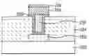
FIGS. 1A to 1F are cross-sectional diagrams of a process of forming a metal line according to a related art, in which a general tungsten plug forming process is applied to forming the metal line.
Referring to FIG. 1A, a metal line 102 is formed on a semiconductor substrate 100 provided with various devices therein. An insulating interlayer 104 is formed over the substrate including the metal line 102 and is then made smooth. A prescribed portion of the insulating interlayer 104 is selectively etched to form a contact or via hole 106 exposing part of the metal line 102.
Referring to FIG. 1B, a first metal layer 108 is formed on the insulating inter layer 104 including an inside of the contact or via hole 106. In this case, the first metal layer 108 is formed of a liner barrier metal such as Ti/TiN.
Referring to FIG. 1C, a tungsten layer 110 is deposited on the first metal layer 108 so that the contact or via hole 106 can be filled up with the tungsten layer 110.
Referring to FIG. 1D, the tungsten layer 110 is etched back to form a tungsten plug 110. After the contact or via hole 106 has been filled up with the tungsten layer 110, CMP (chemical mechanical polishing) is carried out on the tungsten layer 110 and the first metal layer 108. A touch-up process is then carried out on the substrate 100 to remove tungsten residue remaining on the insulating interlayer 104, whereby the tungsten plug 108 filing up the contact or via hole is completed.
Referring to FIG. 1E, a second metal layer 112, a metal layer 114, and a third metal layer 116 are sequentially deposited over the substrate 100 including the tungsten plug. Photoresist is coated on the third metal layer. Exposure and development is carried out on the photoresist to form a photoresist pattern 118 defining a metal line over the tungsten plug. Specifically, the second and third metal layers 112 and 116 are preferably formed of Ti/TiN. The metal layer 114 as a main line material may be formed of aluminum.
Referring to FIG. 1F, dry etch is carried out over the substrate including the third metal layer 116, the metal layer 114, and the second metal layer 112 using the photoresist pattern 118 in FIG. 1E as an etch mask. Hence, a metal line consisting of the second metal layer 112, the metal layer 114, and the third metal layer 116 is completed. Thereafter, the photoresist pattern is removed.
However, in the related art method of forming the metal line, the touch-up process for forming the tungsten plug after CMP for insulating layer smoothing scratches a surface of the insulating interlayer 104 or rips out the insulating interlayer 104 provided with the contact or via hole 106.
SUMMARY OF THE INVENTIONAccordingly, the present invention is directed to a method of forming a metal line in a semiconductor device that substantially obviates one or more problems due to limitations and disadvantages of the related art.
An object of the present invention is to provide a method of forming a metal line in a semiconductor device, which can prevent an insulating layer from ripping out of the device and a scratch from occurring when smoothing a conductive material provided to a contact or via for a metal line.
Another object of the present invention is to provide a method of forming a metal line in a semiconductor device, in which a first metal layer deposited on a insulating interlayer is not completely removed in carrying out CMP after filling a contact or via hole with a conductive material and in which a following metal line forming process is performed on the remaining first metal layer.
Additional advantages, objects, and features of the invention will be set forth in part in the description which follows and in part will become apparent to those having ordinary skill in the art upon examination of the following or may be learned from practice of the invention. The objectives and other advantages of the invention may be realized and attained by the structure particularly pointed out in the written description and claims hereof as well as the appended drawings.
To achieve these objects and other advantages and in accordance with the purpose of the invention, as embodied and broadly described herein, a method of forming a metal line in a semiconductor device according to the present invention includes the steps of forming an insulating interlayer over a substrate provided with a lower metal line, forming a hole exposing the lower metal line, forming a first metal layer on the insulating interlayer including an inside of the hole and the lower metal line, forming a conductor layer on the first metal layer to fill the hole, etching back the conductor layer to form a plug until the first metal layer is exposed, sequentially stacking a second metal layer and a third metal layer on the first metal layer, and patterning the second metal layer, the third metal layer, and the first metal layer to form an upper metal line overlapped with the plug using an etch mask defining the upper metal line.
In an exemplary embodiment, the method further includes the step of removing the etch mask.
In an exemplary embodiment, the first and second metal layers are each formed of Ti/TiN.
In an exemplary embodiment, the metal layer is formed of aluminum.
In an exemplary embodiment, the conductor layer is formed of tungsten.
In an exemplary embodiment, the etching back step includes chemical mechanical polishing (CMP).
It is to be understood that both the foregoing general description and the following detailed description of the present invention are exemplary, but are not restrictive of the invention.
BRIEF DESCRIPTION OF THE DRAWINGSThe accompanying drawings, which are included to provide a further understanding of the invention and are incorporated in and constitute a part of this application, illustrate embodiment(s) of the invention and together with the description serve to explain the principle of the invention. In the drawings:
FIGS. 1A to 1F are cross-sectional diagrams for explaining a process of forming a metal line according to a related art; and
FIGS. 2A to 2F are cross-sectional diagrams for explaining a process of forming a metal line in a semiconductor device according to an exemplary embodiment of the present invention.
DETAILED DESCRIPTION OF THE INVENTIONReference will now be made in detail to exemplary embodiments of the present invention, which are illustrated in the accompanying drawings. Wherever possible, the same reference numbers will be used throughout the drawings to refer to the same or like parts.
An exemplary embodiment of the present invention is characterized as follows. A first metal layer deposited on an insulating interlayer is not completely removed after carrying out CMP after filling a contact or via hole with a conductive material. A metal line forming process is performed on the remaining first metal layer.
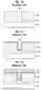
FIGS. 2A to 2F are cross-sectional diagrams for explaining a process of forming a metal line in a semiconductor device according to an exemplary embodiment of the present invention.
Referring to FIG. 2A, a metal line 202 is formed on a semiconductor substrate 200 provided with various devices therein. Subsequently, an insulating interlayer 204 is formed over the semiconductor substrate 200 including the metal line 202 and is then made smooth. A prescribed portion of the insulating interlayer 204 is selectively etched to form a contact or via hole 206 exposing part of the metal line 202.
Referring to FIG. 2B, a first metal layer 208 is formed on the insulating inter layer 204 including an inside of the contact or via hole 206. In this case, the first metal layer 208 is formed of a liner barrier metal such as Ti/TiN.
Referring to FIG. 2C, a tungsten layer 210 is deposited on the first metal layer 208 so that the contact or via hole 206 is filled up with the tungsten layer 210.
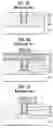
Referring to FIG. 2D, the tungsten layer 210 is etched back to form a tungsten plug 210 within the contact or via hole. Specifically, in carrying out CMP (chemical mechanical polishing) after the contact or via hole 206 has been filled up with the tungsten layer 210, the first metal layer 208 is used as a CMP-stop layer. Namely, CMP is carried out until a surface of the first metal layer 208 is exposed. Hence, the first metal layer 208 is not completely removed but remains on the insulating interlayer 204.
Referring to FIG. 2E, a second metal layer 214 and a third metal layer 216 are sequentially deposited over the substrate 200 including the tungsten plug 210. Photoresist is coated on the third metal layer 216. Exposure and development is carried out on the photoresist to form a photoresist pattern 218 defining a metal line over the tungsten plug 210. Specifically, the third metal layer 216 is preferably formed of Ti/TiN. And, the second metal layer 214 as a main line material may be formed of aluminum.
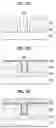
Referring to FIG. 2F, dry etch is carried out over the substrate 200 including the third metal layer 216, the second metal layer 214, and the first metal layer 208 using the photoresist pattern 218 in FIG. 2E as an etch mask. Hence, a metal line consisting of the first metal layer 208, the second metal layer 214, and the third metal layer 216 is completed over the tungsten plug 210. Finally, the photoresist pattern is removed.
Accordingly, in the present invention, the related art touch-up process can be skipped in forming the metal line of the semiconductor device, whereby an overall process can be simplified. Further, the present invention can prevent the scratches and damage caused to the insulating interlayer.
Moreover, the first metal layer is overetched in patterning the metal line on the insulating interlayer so that tungsten residues can be efficiently removed from the surface of the first metal layer.
Therefore, the present invention lowers failure in forming the metal line, thereby enhancing reliability and yield of the semiconductor devices.
Korean Patent Application No. P2003-0089431, filed on Dec. 10, 2003, is incorporated herein by reference in its entirety.
It will be apparent to those skilled in the art that various modifications and variations can be made in practicing the present invention. Thus, it is intended that the present invention covers the modifications and variations of this invention within the scope of the appended claims and their equivalents.
Claims
1. A method of forming a metal line in a semiconductor device, comprising the steps of:
forming an insulating interlayer over a substrate provided with a lower metal line;
forming a hole exposing the lower metal line;
forming a first metal layer on the insulating interlayer including an inside of the hole and the lower metal line;
forming a conductor layer on the first metal layer to fill the hole;
etching back the conductor layer to form a plug until the first metal layer is exposed;
sequentially stacking a second metal layer and a third metal layer on the first metal layer; and
patterning the second metal layer, the third metal layer, and the first metal layer to form an upper metal line overlapped with the plug using an etch mask defining the upper metal line.
2. The method of claim 1, further comprising the step of removing the etch mask.
3. The method of claim 1, wherein the first and second metal layers are each formed of Ti/TiN.
4. The method of claim 1, wherein the metal layer is formed of aluminum.
5. The method of claim 1, wherein the conductor layer is formed of tungsten.
6. The method of claim 1, wherein the etching back step includes chemical mechanical polishing.
7. A method of forming a metal line in a semiconductor device, comprising:
a step for forming an insulating interlayer over a substrate provided with a lower metal line;
a step for forming a hole exposing the lower metal line;
a step for forming a first metal layer on the insulating interlayer including an inside of the hole and the lower metal line;
a step for forming a conductor layer on the first metal layer to fill the hole;
a step for etching back the conductor layer to form a plug until the first metal layer is exposed;
a step for sequentially stacking a second metal layer and a third metal layer on the first metal layer; and
a step for patterning the second metal layer, the third metal layer, and the first metal layer to form an upper metal line overlapped with the plug using an etch mask defining the upper metal line.
8. The method of claim 7, further comprising a step for removing the etch mask.
9. The method of claim 7, wherein the first and second metal layers are each formed of Ti/TiN.
10. The method of claim 7, wherein the metal layer is formed of aluminum.
11. The method of claim 7, wherein the conductor layer is formed of tungsten.
12. The method of claim 7, wherein the step for etching back includes chemical mechanical polishing.
Images & Drawings included:

Sources:
- United States Patent and Trademark Office - verify current appl. status at the USPTO↗
Similar patent applications:
- » 20240266291
MATERIAL FOR METAL LINE, METAL LINE IN SEMICONDUCTOR DEVICE AND METHOD FOR FORMING METAL LINE IN SEMICONDUCTOR DEVICE - » 20240194604
MATERIAL FOR METAL LINE IN SEMICONDUCTOR DEVICE, METAL LINE IN SEMICONDUCTOR DEVICE, AND METHOD FOR FORMING METAL LINE IN SEMICONDUCTOR DEVICE - » 20060046466
Semiconductor device and method for forming a metal line in the semiconductor device - » 20050142857
Method for forming metal line in semiconductor device - » 10749650
Methods of forming metal lines in semiconductor devices - » 10744494
Method of forming metal line in semiconductor device including forming first and second zirconium films - » 20050014384
Method of forming metal line in semiconductor device - » 20050009321
Method of forming metal line in semiconductor device - » 10735228
Method of forming metal line of semiconductor device - » 10746652
Methods of forming metal lines in semiconductor devices
Recent applications in this class:
- » 20240258163 2024-08-01
MITIGATING PATTERN COLLAPSE - » 20240021470 2024-01-18
SEMICONDUCTOR DEVICE AND MANUFACTURING METHOD THEREFOR - » 20230178428 2023-06-08
LEADED SEMICONDUCTOR PACKAGE FORMATION USING LEAD FRAME WITH STRUCTURED CENTRAL PAD - » 20220199464 2022-06-23
Semiconductor device protection using an anti-reflective layer - » 20210313225 2021-10-07
3D IC method and device - » 20210296166 2021-09-23
Stress analysis method and semiconductor device manufacturing method - » 20210280461 2021-09-09
3D IC method and device - » 20210202306 2021-07-01
Mitigating pattern collapse - » 20210090945 2021-03-25
SYSTEM AND METHOD FOR INTERCONNECTION - » 20200357689 2020-11-12
Adjusting reactive components
Recent applications for this Assignee:
- » 20100314675 2010-12-16
Power semiconductor device and method for manufacturing the same - » 20100133421 2010-06-03
Complementary metal oxide silicon image sensor and method of fabricating the same - » 20100029051 2010-02-04
Semiconductor device and fabricating method thereof - » 20100019353 2010-01-28
Semiconductor device and method for manufacturing the same - » 20090317953 2009-12-24
Memory device and method for manufacturing the same - » 20090317952 2009-12-24
Memory device and method for manufacturing the same - » 20090317949 2009-12-24
ESD protecting circuit and manufacturing method thereof - » 20090302361 2009-12-10
Complementary metal oxide semiconductor (CMOS) image sensor - » 20090278205 2009-11-12
High voltage BICMOS device and method for manufacturing the same - » 20090273032 2009-11-05
LDMOS device and method for manufacturing the same