Method of forming a salicide layer for a semiconductor device
US20050142736A1
2005-06-30
11/027,076
2004-12-29
✅ Patent granted
US 7,550,373 B2
2009-06-23
-
-
Jack Chen
2024-12-29
Abstract:
Methods of fabricating semiconductor devices are disclosed. An illustrated example method protects spacers and active areas by performing impurity ion implantation on an oxide layer prior to etching the oxide layer. The illustrated method includes forming a gate on a semiconductor substrate, forming a spacer on a sidewall of the gate, forming an oxide layer over the substrate, forming a mask on the oxide layer to cover a non-salicide area, implanting impurity ions into a portion of the oxide layer which is not covered by the mask, removing the portion of the oxide layer which is implanted with impurity ions, performing salicidation on the substrate, and removing the mask.
Assignee:
- Dongbu Electronics Co., Ltd. 766 🇰🇷 Seoul, South Korea
Interested in similar patents?
Get notified when new applications in this technology area are published.
Classification:
H01L21/3205 IPC
Processes or apparatus adapted for the manufacture or treatment of semiconductor or solid state devices or of parts thereof; Manufacture or treatment of semiconductor devices or of parts thereof the devices having at least one potential-jump barrier or surface barrier, e.g. PN junction, depletion layer or carrier concentration layer the devices having semiconductor bodies comprising elements of Group IV of the Periodic System or AB compounds with or without impurities, e.g. doping materials; Treatment of semiconductor bodies using processes or apparatus not provided for in groups - to form insulating layers thereon, e.g. for masking or by using photolithographic techniques ; After treatment of these layers; Selection of materials for these layers Deposition of non-insulating-, e.g. conductive- or resistive-, layers on insulating layers; After-treatment of these layers
Description
FIELD OF THE DISCLOSUREThe present disclosure relates generally to semiconductor fabrication and, more particularly, to methods of fabricating semiconductor devices in which a non-silicide or non-salicide area is protected when forming a salicide layer in order to secure a resistance of the protected area.
BACKGROUNDGenerally, in order to lower the resistance of a polysilicon gate electrode to accommodate a decrease in a critical dimension in CMOS device fabrication, a silicide layer is formed on the gate electrode. Since silicidation or salicidation is an optional process, a non-silicide or non-salicide area having no silicide may be formed on a specific portion of a device that requires higher resistance then the gate electrode.
A prior art method of forming a non-salicide area includes: forming a gate and spacers on a semiconductor substrate, forming an oxide layer thereon, forming a photoresist pattern covering an area that is not to be covered with salicide, removing the portions of the oxide layer which are not covered by the photoresist pattern, and forming a Ti- or Co-silicide layer on the uncovered areas. Thus, the non-salicide area is formed by preventing the silicide layer from being formed on the area covered by the photoresist pattern. The oxide layer is etched by wet etching, plasma dry etching (e.g., anisotropic etching), or by wet and dry etching using the photoresist pattern as an etch mask.
However, in the prior art method, if the oxide layer is wet etched, the etchant solution undercuts beneath the spacers. If, on the other hand, dry etching is performed, plasma damage occurs. Consequently, gate leakage is generated or the threshold voltage of the fabricated transistor is changed.
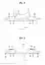
BRIEF DESCRIPTION OF THE DRAWINGSFIGS. 1 to 9 are cross-sectional views illustrated an example method of fabricating a semiconductor device performed in accordance with the teachings of the present invention.
Wherever possible, the same reference numbers will be used throughout the drawings to refer to the same or like parts.
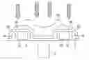
DETAILED DESCRIPTIONFIGS. 1 to 9 are cross-sectional views illustrating example methods of fabricating a semiconductor device constructed in accordance with the teachings of the present invention. Referring to FIG. 1, an STI (shallow trench isolation) layer 2 is formed in a silicon substrate 1 to define left and right active areas in the silicon substrate 1.
Referring to FIG. 2, an insulating layer is formed on the substrate 1. A polysilicon layer is then deposited on the insulating layer.
The polysilicon and insulating layers are patterned by photolithography to form a pair of gate electrodes 21 and 22 on the left and right active areas, respectively. Gate insulating layers 11 and 12 are located underneath respective ones of the gate electrodes 21 and 22.
Referring to FIG. 3, a first oxide layer 30 is formed as a protective layer on the substrate 1 and the gate electrodes 21 and 22. Optionally, the protective layer 30 can be formed of a double layer including an oxide layer and a TEOS layer.
Referring to FIG. 4, a nitride (SiN) layer is formed on the first oxide layer 30. The nitride layer is etched back to form spacers 41 and 42 on sidewalls of the gate electrodes 21 and 22, respectively.
Referring to FIG. 5, a second oxide layer 50 is formed on the spacers 41 and 42 and on the first oxide layer 30.
Referring to FIG. 6, a photoresist layer is coated on the second oxide layer 50. The photoresist layer is selectively exposed and developed to form a photoresist pattern 60 covering only a non-salicide area.
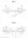
Referring to FIG. 7, impurity ions are implanted in the substrate 1 including in the second oxide layer 50. In the illustrated example, the implanted impurity ion species are Ge, As, BF2, Ar, P, In, Sb, and/or the like. In the illustrated example, the implantation process is performed at a dose of about 1E12˜1E16 ions/cm2 with an implantation energy of about 5˜160 KeV.
Referring to FIG. 8, wet etching is performed on the substrate using the photoresist pattern 60 as an etch mask to remove portions of the oxide layers 30 and 50, thereby exposing salicide forming areas, (e.g., the topsides of the gate electrodes 21 and 22 and portions of the active areas of the substrate 1).
Since the ion implantation process is performed prior to wet etching the first and second oxide layers 30 and 50, the coherence of the oxide layers is weakened, thereby accelerating their etch rates during the wet etching process. As a result, the time taken for the spacers 41 and 42 and the active areas to be exposed by an etchant solution is reduced. Therefore, the undercut between the spacer 41 or 42 and the active areas of the substrate 1 can be minimized.
The removal of the oxide layers 30 and 50 for salicidation may be performed by plasma dry etching (e.g., anisotropic etching), by wet etching, or by mixed dry and wet etching. If dry etching is performed, the ion implantation is performed after completion of the dry etching, (i.e., after the process described in connection with FIG. 8). If mixed dry and wet etching is performed, the dry etching, ion implantation, and wet etching are executed in the order listed in this sentence. Since the ion implantation is performed after dry etching, impurity ions penetrate the active areas damaged by the dry etching process to help salicidation.
Referring to FIG. 9, a metal layer of Ti, Co, or the like is deposited over the substrate 1 including over the exposed topsides of the gates 21 and 22 and the exposed active areas of the substrate 1. This metal layer is then annealed to form a salicide layer 70. The portion of the metal layer which fails to react with the silicon is removed.
Thereafter, the photoresist pattern is removed to open a non-salicide area 80.
From the foregoing, persons of ordinary skill in the art will appreciate that, by performing the ion implantation prior to wet etching to selectively remove the oxide layers, the coherence of the oxide layers is weakened and their etch rates are accelerated in the subsequent wet etching process. As a result, the time taken for the spacers and the active areas to be exposed by an etchant solution is reduced. Consequently, the undercut between the spacers and the active areas of the substrate 1 can be minimized.
Moreover, because the additional ion implantation is performed after dry etching, impurity ions penetrate the active areas damaged by the dry etching process to help salicidation. Consequently, separate ion implantation is unnecessary for salicidation.
From the foregoing, persons of ordinary skill in the art will readily appreciate that methods of fabricating semiconductor devices have been disclosed by which spacers and active areas are protected by performing impurity ion implantation on an oxide layer prior to etching the oxide layer.
A disclosed example method of fabricating a semiconductor device comprises: forming a gate having a gate insulating layer on a semiconductor substrate, forming a spacer on a sidewall of the gate, forming an oxide layer over the substrate, forming a mask on the oxide layer to cover a non-salicide area, implanting impurity ions into an area of the oxide layer which is not covered by the mask, removing the area of the oxide layer which is implanted with impurity ions, performing salicidation on the substrate, and removing the mask.
Preferably, the area of the oxide layer which is implanted with impurity ions is removed by wet etching.
Preferably, the mask is formed of a photoresist pattern.
Another disclosed example method of fabricating a semiconductor device comprises: forming a gate having a gate insulating layer on a semiconductor substrate, forming a spacer on a sidewall of the gate, forming an oxide layer over the substrate, forming a mask on the oxide layer to cover a non-salicide area, removing a portion of the oxide layer which is not covered by the mask by dry etching, performing ion implantation on the substrate, performing salicidation on the substrate, and removing the mask.
Preferably, the impurity ions comprise at least one of Ge, As, BF2, Ar, P, In, or Sb.
Preferably, the ion implantation is performed at a dose of about 1E121E16 ions/cm2 with implantation energy of about 5˜160 KeV.
Preferably, the salicidation is performed using Ti or Co.
It is noted that this patent claims priority from Korean Patent Application Serial Number P2003-0100951, which was filed on Dec. 30, 2003, and is hereby incorporated by reference in its entirety.
Although certain example methods, apparatus and articles of manufacture have been described herein, the scope of coverage of this patent is not limited thereto. On the contrary, this patent covers all methods, apparatus and articles of manufacture fairly falling within the scope of the appended claims either literally or under the doctrine of equivalents.
Claims
1. A method of fabricating a semiconductor device comprising:
forming a gate on a semiconductor substrate;
forming a spacer on a sidewall of the gate;
forming an oxide layer;
forming a mask on the oxide layer to cover a non-salicide area;
implanting impurity ions into a portion of the oxide layer which is not covered by the mask;
removing the portion of the oxide layer which is implanted with the impurity ions;
performing salicidation on the substrate; and
removing the mask.
2. A method as defined in claim 1, wherein removing the portion of the oxide layer which is implanted with the impurity ions comprises wet etching the portion of the oxide layer.
3. A method as defined in claim 1, wherein the mask comprises a photoresist pattern.
4. A method of fabricating a semiconductor device comprising:
forming a gate on a semiconductor substrate;
forming a spacer on a sidewall of the gate;
forming an oxide layer over the substrate;
forming a mask on the oxide layer to cover a non-salicide area;
dry etching a portion of the oxide layer which is not covered with the mask;
performing ion implantation on the substrate;
performing salicidation on the substrate; and
removing the mask.
5. A method as defined in claim 4, wherein the impurity ions comprise at least one of Ge, As, BF2, Ar, P, In, or Sb.
6. A method as defined in claim 4, wherein the ion implantation is performed at a dose of about 1E12˜1E16 ions/cm2 at an implantation energy of about 5˜160 KeV.
7. A method as defined in claim 4, wherein the salicidation is performed using Ti or Co.
Images & Drawings included:
Sources:
- United States Patent and Trademark Office - verify current appl. status at the USPTO↗
Similar patent applications:
- » 20060148228
Method for forming salicide layer in semiconductor device - » 20080299767
Method for Forming a Semiconductor Device Having a Salicide Layer - » 20090221121
Method of forming a salicide layer for a semiconductor device - » 20190131421
Semiconductor device structure with salicide layer and method for forming the same - » 20050196945
Methods of forming a double metal salicide layer and methods of fabricating semiconductor devices incorporating the same
Recent applications in this class:
- » 20250293040 2025-09-18
SUBSTRATE PROCESSING METHOD AND SUBSTRATE PROCESSING APPARATUS - » 20250293039 2025-09-18
METHODS FOR WET ATOMIC LAYER ETCHING OF SILICON DIOXIDE - » 20250210366 2025-06-26
MANUFACTURING METHOD OF SEMICONDUCTOR DEVICE - » 20250201572 2025-06-19
METHODS FOR WET ATOMIC LAYER ETCHING OF TRANSITION METAL OXIDE DIELECTRIC MATERIALS - » 20250183050 2025-06-05
METHOD FOR TREATING OBJECT TO BE TREATED, TREATMENT LIQUID, AND METHOD FOR MANUFACTURING ELECTRONIC DEVICE - » 20250183049 2025-06-05
CHEMICAL SOLUTION, ETCHING METHOD, AND METHOD FOR MANUFACTURING SEMICONDUCTOR DEVICE - » 20250132164 2025-04-24
SUBSTRATE PROCESSING METHOD AND SUBSTRATE PROCESSING APPARATUS - » 20250125154 2025-04-17
OXIDE QUALITY DIFFERENTIATION - » 20250079180 2025-03-06
METHODS FOR WET ATOMIC LAYER ETCHING OF MOLYBDENUM - » 20250062132 2025-02-20
Etching method of semiconductor structure
Recent applications for this Assignee:
- » 20100314675 2010-12-16
Power semiconductor device and method for manufacturing the same - » 20100133421 2010-06-03
Complementary metal oxide silicon image sensor and method of fabricating the same - » 20100029051 2010-02-04
Semiconductor device and fabricating method thereof - » 20100019353 2010-01-28
Semiconductor device and method for manufacturing the same - » 20090317953 2009-12-24
Memory device and method for manufacturing the same - » 20090317952 2009-12-24
Memory device and method for manufacturing the same - » 20090317949 2009-12-24
ESD protecting circuit and manufacturing method thereof - » 20090302361 2009-12-10
Complementary metal oxide semiconductor (CMOS) image sensor - » 20090278205 2009-11-12
High voltage BICMOS device and method for manufacturing the same - » 20090273032 2009-11-05
LDMOS device and method for manufacturing the same