Conductive pattern producing method and its applications
US20050148165A1
2005-07-07
11/048,767
2005-02-03
✅ Patent granted
US 7,288,437 B2
2007-10-30
-
-
Wael Fahmy | Pamela E Perkins
2025-02-03
Abstract:
An improved method of forming an electrode pattern on a substrate is described. The substarate is coated with a first conductive film and subjected to baking. On the first conductive film is then overlied a second conductive film which mends possible fissures of the first conductive film which, besides, would produce open circuits in the pattern.
Assignee:
- SEMICONDUCTOR ENERGY LABORATORY CO., LTD. 7,025 🇯🇵 Kanagawa-ken, Japan
- Semiconductor Energy Laboratory 3 🇯🇵 Atsugi-shi, Japan
Interested in similar patents?
Get notified when new applications in this technology area are published.
Classification:
H01L2924/00011 » CPC further
Indexing scheme for arrangements or methods for connecting or disconnecting semiconductor or solid-state bodies as covered by; Technical content checked by a classifier Not relevant to the scope of the group, the symbol of which is combined with the symbol of this group
H01L2224/29075 » CPC further
Indexing scheme for arrangements for connecting or disconnecting semiconductor or solid-state bodies and methods related thereto as covered by; Means for bonding being attached to, or being formed on, the surface to be connected, e.g. chip-to-package, die-attach, "first-level" interconnects; Manufacturing methods related thereto; Layer connectors, e.g. plate connectors, solder or adhesive layers; Manufacturing methods related thereto; Structure, shape, material or disposition of the layer connectors prior to the connecting process of an individual layer connector; Core members of the layer connector Plural core members
H01L2224/83851 » CPC further
Indexing scheme for arrangements for connecting or disconnecting semiconductor or solid-state bodies and methods related thereto as covered by; Methods for connecting semiconductor or other solid state bodies using means for bonding being attached to, or being formed on, the surface to be connected using a layer connector; Bonding techniques using a polymer adhesive, e.g. an adhesive based on silicone, epoxy, polyimide, polyester being an anisotropic conductive adhesive
H01L2924/00014 » CPC further
Indexing scheme for arrangements or methods for connecting or disconnecting semiconductor or solid-state bodies as covered by; Technical content checked by a classifier the subject-matter covered by the group, the symbol of which is combined with the symbol of this group, being disclosed without further technical details
G02F1/13452 » CPC main
Devices or arrangements for the control of the intensity, colour, phase, polarisation or direction of light arriving from an independent light source, e.g. switching, gating or modulating; Non-linear optics for the control of the intensity, phase, polarisation or colour based on liquid crystals, e.g. single liquid crystal display cells; Constructional arrangements; Operation of liquid crystal cells; Circuit arrangements; Constructional arrangements; Manufacturing methods; Conductors connecting electrodes to cell terminals Conductors connecting driver circuitry and terminals of panels
G02F1/13439 » CPC further
Devices or arrangements for the control of the intensity, colour, phase, polarisation or direction of light arriving from an independent light source, e.g. switching, gating or modulating; Non-linear optics for the control of the intensity, phase, polarisation or colour based on liquid crystals, e.g. single liquid crystal display cells; Constructional arrangements; Operation of liquid crystal cells; Circuit arrangements; Constructional arrangements; Manufacturing methods; Electrodes characterised by their electrical, optical, physical properties; materials therefor; method of making
G02F1/1345 » CPC further
Devices or arrangements for the control of the intensity, colour, phase, polarisation or direction of light arriving from an independent light source, e.g. switching, gating or modulating; Non-linear optics for the control of the intensity, phase, polarisation or colour based on liquid crystals, e.g. single liquid crystal display cells; Constructional arrangements; Operation of liquid crystal cells; Circuit arrangements; Constructional arrangements; Manufacturing methods Conductors connecting electrodes to cell terminals
H01L21/4867 » CPC further
Processes or apparatus adapted for the manufacture or treatment of semiconductor or solid state devices or of parts thereof; Manufacture or treatment of semiconductor devices or of parts thereof the devices having at least one potential-jump barrier or surface barrier, e.g. PN junction, depletion layer or carrier concentration layer; Manufacture or treatment of parts, e.g. containers, prior to assembly of the devices, using processes not provided for in a single one of the subgroups -; Conductive parts; Leads on or in insulating or insulated substrates, e.g. metallisation Applying pastes or inks, e.g. screen printing
H05K3/245 » CPC further
Apparatus or processes for manufacturing printed circuits; Secondary treatment of printed circuits; Reinforcing the conductive pattern Reinforcing conductive patterns made by printing techniques or by other techniques for applying conductive pastes, inks or powders; Reinforcing other conductive patterns by such techniques
H01L2224/81192 » CPC further
Indexing scheme for arrangements for connecting or disconnecting semiconductor or solid-state bodies and methods related thereto as covered by; Methods for connecting semiconductor or other solid state bodies using means for bonding being attached to, or being formed on, the surface to be connected using a bump connector; Arrangement of the bump connectors prior to mounting wherein the bump connectors are disposed only on another item or body to be connected to the semiconductor or solid-state body
H05K1/095 » CPC further
Printed circuits; Details; Use of materials for the conductive, e.g. metallic pattern; Dispersed materials, e.g. conductive pastes or inks for polymer thick films, i.e. having a permanent organic polymeric binder
H05K1/095 » CPC further
Printed circuits; Details; Use of materials for the conductive, e.g. metallic pattern; Dispersed materials, e.g. conductive pastes or inks for polymer thick films, i.e. having a permanent organic polymeric binder
H05K2201/0326 » CPC further
Indexing scheme relating to printed circuits covered by; Conductive materials; Materials Inorganic, non-metallic conductor, e.g. indium-tin oxide [ITO]
H05K2201/0326 » CPC further
Indexing scheme relating to printed circuits covered by; Conductive materials; Materials Inorganic, non-metallic conductor, e.g. indium-tin oxide [ITO]
H05K2201/035 » CPC further
Indexing scheme relating to printed circuits covered by; Conductive materials; Structure of the conductor; Layered conductors or foils Paste overlayer, i.e. conductive paste or solder paste over conductive layer
H05K2201/035 » CPC further
Indexing scheme relating to printed circuits covered by; Conductive materials; Structure of the conductor; Layered conductors or foils Paste overlayer, i.e. conductive paste or solder paste over conductive layer
Y10T29/4913 » CPC further
Metal working; Method of mechanical manufacture; Electrical device making; Conductor or circuit manufacturing; On flat or curved insulated base, e.g., printed circuit, etc. Assembling to base an electrical component, e.g., capacitor, etc.
Y10T29/49137 » CPC further
Metal working; Method of mechanical manufacture; Electrical device making; Conductor or circuit manufacturing; On flat or curved insulated base, e.g., printed circuit, etc.; Assembling to base an electrical component, e.g., capacitor, etc. with component orienting Different components
Y10T29/49155 » CPC further
Metal working; Method of mechanical manufacture; Electrical device making; Conductor or circuit manufacturing; On flat or curved insulated base, e.g., printed circuit, etc. Manufacturing circuit on or in base
H01L21/00 IPC
Processes or apparatus adapted for the manufacture or treatment of semiconductor or solid state devices or of parts thereof
Description
BACKGROUND OF THE INVENTIONThis invention relates to a conductive pattern producing method, and more particularly, relates to an improvement for conductive pattern producing method which makes the pattern thus produced by the method more credible.
Heretofore, the interest of operators to manufacture liquid crystal devices which comprises a pair of glass substrates and electrode pattern including addressing lines and signal lines for producing a matrix arragement, is directed to how to form a pattern on the substrates without deffect and with a high reliability of the pattern. Also the device generally includes an IC chip for driving the liquid crystal device. The facilitataion and credibility of the connection between the IC chip and the pattern is alway in question. Particularly, in the case that a pattern is formed on a glass substrate, there likely occur fissures in the pattern which cause disconnection of circuitry.
SUMMARY OF THE INVENTIONIt is therefore an object of the invention to provide a method for producing a credible pattern.
In order to accomplish the object of the invention, patterns are manufactured with double-layered film.
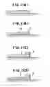
BRIEF DESCRIPTION OF THE INVENTIONFIGS. 1(A) to 1(D) are cross sectional views showing a method of manufacturing a conductive pattern in accordance with the present invention.
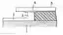
FIGS. 2(A) and 2(B) are a plan view and cross sectional partial view showing a pattern fromed in accordance with the present invention.
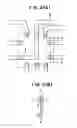
FIGS. 3(A) and 3(B) are cross sectional partial views showing contact portions between IC chips and conductive patterns in accordance with the present invention.
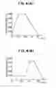
FIGS. 4(A) and 4(B) are graphical diagrams of temperature curves which are used in methods in accordance with the present invention.
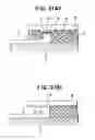
FIGS. 5(A) to 5(C) are cross sectional views showing a method in accordance with the present invention.
FIG. 6 is a cross sectional view showing the contact portion between an IC chip and the conductive pattern produced by the method as illustrated in FIGS. 5(A) to 5(C).
DETAILED DESCRIPTION OF THE PREFERRED EMBODIMENTSReferring to FIGS. 1(A) to 1(D), a method of forming a conductive pattern on a substrate for mounting thereon an IC chip in accordance with the present invention. On a glass substrate for liquid crystal device, only a portion of which is illustrated in the figures, a conductive pattern is formed by offset screen printing with a conductive paste (FIG. 1(A)). The conductive paste for the pattern is prepared by mixing, with an oil emulsion, “cover silver paste” (Prod No. 61900234) distributed by Detmeron, a manufacture of FRG. The thickness of the pattern is 10 microns. Then, the substrate is baked in a nitrogen atmosphere in accordance with a temperature curve shown in FIG. 4(A), so that formed are a contact region 2a and a sintered region largely consisting of silver (FIG. 1(B)). Also, on a portion of the pattern, another pattern to make a thick portion is formed in the same manner by printing and baking (FIGS. 1(C) and 1(D)). The thickness of the thick portion is 30 microns after baking. Instead of printing, the pattern can be formed of ITO by sputtering with a good contact and a good conductivity. FIGS. 2(A) and 2(B) are plan view and a cross sectional view showing the whole pattern on the substrate formed as explaned above.
After the formation of the pattern, a transparent adhesive of epoxy resin mixed with Ni particles having 15 microns in average diameter is applied to the surface of the substrate which is to face the bottom surface and the electrode pads of an IC. The Ni particles are added into at 50 mg per each 5 g of the adhesive. Then, the IC chip is mounted on the substrate with its aluminium pads contacting corresponding pads of the thick portion of the pattern, and the epoxy resin is hardened at 180° C. while pressing the IC against the substrate for 20 munites with a force of 3 Kg using a jig. During the mounting of the IC chip, the alignment of the pads of the IC chip with the pattern on the substrate is checked by viewing the both from the bottom of the substrate through the transparent resin.
A resin which can be cured by a UV light may be also used as the adhesive. In this alternative, the resin is irradiated with a UV light through the transparent substrate.
FIG. 3(A) is a partial cross section view showing the contact of the IC chip 5 with the substrate 1 after the hardening of the epoxy adhesive. The distance between the Al pad 8 and the top of the thick portion 3 is designed 3 microns in which the Ni particles are caught and make the resistance of the contact low. Other particles contained in the epoxy resin are situated between the IC chip and the substrate with 30 microns in distance, and do not damage the IC chip and the pattern 2 on the substrate 1. The area of the thick portion is preferably smaller than that of the corresponding pad of the pattern.
Next, a second embodiment of the invention is described. After the formation of the pattern by printing and baking in the same manner as the pattern 2 of the preceding embodiment, a thick portion 3 is formed by coating the prescribed portion with DAP1 (No. 61901143), a conductive adhesive distributed by Detmeron. Then, the IC chip is mounted on the substrate with its aluminium pads contacting corresponding lands of the thick portion of the pattern and pressed against the substrate with a jig, and the substrate is baked in accordance with the temperature curve shown in FIG. 4(B). FIG. 3(B) is a cross sectional view showing the electrical connection between the IC chip and the pattern in accordance with this embodiment. By this embodiment, the method of the present invention brings the advantage that a few number of processing steps are required for mounting an IC chip and making necessary contact with the IC chip.
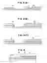
Referring to FIGS. 5(A) to 5(C), a third embodiment of the invention is illustrated. In FIG. 5(A), a glass substrate 1 is coated by printing with a conductive paste consisting of Cu particles dispersed in a phenol resin, in order to form a prescribed pattern 11 inclusing electrode lines for making contact with counterpart pads of the IC chip. The average diameter of the Cu particle is 5-10 microns. This conductive paste coating is then baked at 60° C. for 10 munites and becomes thin by shrinking. The baked layer 11 might have a fissure 12.
Then, another layer 13 of the Cu conductive paste is superimposed over the layer 11 by printing on the baked Cu layer as shown in FIG. 5(B). The overlying Cu layer is also baked at 60° C. for 10 munites. The fissure 12 has to be mended by this overlying pattern. The dispersion of the double-layered pattern in thickness is about 30 microns. The double-layered pattern is then pressed to produce an even top surface 14. The thickness of the double-layered pattern becomes about 20 microns after pressing. On the pattern is mounted an IC chip whose electrode pads to be made contact with the patterns are given Au bumps by plating and the IC chip is pressed against the substrate with an adhesive resin securing the IC chip in place.
While a description has been made for several embodiments, the present invention should be limited only by the appended claims and should not be limited by the particualr examles.
Claims
1. A method for manufacturing a semiconductor device comprising the steps of:
forming a conductive pattern on an insulating surface over a substrate;
forming a conductive projection at a predetermined position on said conductive pattern;
mounting a semiconductor chip on said substrate utilizing a curable adhesive having conductive particles within the adhesive such that when said substrate and projection are adhered to the semiconductor chip, a conductive pad of said chip is electrically connected to said projection by said particles within said adhesive; and
curing said adhesive.
2. The method of claim 1, wherein the mounting step includes providing the curable adhesive having metal particles therein between the chip and the substrate, between the projection and the pad of the chip, and between the chip and the conductive pattern.
3. The method of claim 1, wherein the metal particles include nickel.
4. The method of claim 1, wherein said conductive pattern is formed of ITO.
5. The method of claim 1, wherein said conductive projection is formed by printing with a conductive paste.
6. The method of claim 5, further including the step of baking said conductive paste after printing.
7. The method of claim 1, wherein said semiconductor chip is an IC chip.
8. The method of claim 7, wherein said IC chip is an IC chip which drives a liquid crystal device.
9. The method of claim 1 wherein said semiconductor chip and said conductive pattern at least partly overlap each other.
10. The method of claim 9 wherein the gap between said conductive pattern and said semiconductor chip is larger than the diameter of said conductive particles.
11. A method for manufacturing a semiconductor device comprising the steps of:
forming a conductive pattern on an insulating surface over a substrate;
forming a conductive projection by printing at a predetermined position on said conductive pattern by applying a conductive paste including first metal particles;
placing an adhesive on a portion of said substrate, said adhesive including an organic resin having second metal particles therein;
mounting a semiconductor chip on said substrate, such that said organic resin bonds a conductive pad of said chip and said conductive projection; and
curing the organic resin.
12. The method of claim 11, wherein said metal particles comprise nickel.
13. The method of claim 11, wherein said conductive projection is formed by printing with a conductive paste.
14. The method of claim 11, wherein said conductive pattern is formed of ITO.
15. The method of claim 11, wherein said semiconductor chip is an IC chip.
16. The method of claim 11 wherein said semiconductor chip and said conductive pattern at least partly overlap each other.
17. The method of claim 11 wherein said semiconductor device is a liquid crystal device.
19. A method of manufacturing a semiconductor device comprising the steps of:
printing a resin paste loaded with metal particles in accordance with a prescribed pattern;
baking said resin paste;
forming a laminate conductive pattern by repeating said printing and baking steps; and
pressing the laminate conductive pattern in order to produce an even top surface.
20. The method of claim 19 wherein the metal particles comprise copper particles.
21. The method of claim, 19 further comprising the step of:
plating gold pads on the laminate conductive pattern, and
mounting an IC chip in the gold pads in electrical connection, therewith.
Images & Drawings included:
Sources:
- United States Patent and Trademark Office - verify current appl. status at the USPTO↗
Recent applications in this class:
- » 20250258410 2025-08-14
DISPLAY DEVICE - » 20250251634 2025-08-07
DISPLAY DEVICE HAVING CONNECTION UNIT - » 20250251633 2025-08-07
ELECTRONIC DEVICE - » 20250216727 2025-07-03
DISPLAY PANEL AND DISPLAY APPARATUS INCLUDING THE SAME - » 20250172841 2025-05-29
Variable Pitch Fan-out Routing for Display Panels Having Narrow Borders - » 20250155756 2025-05-15
DISPLAY UNIT HAVING A CURVED DISPLAY PANEL - » 20250147366 2025-05-08
Electronic device - » 20250130464 2025-04-24
ELECTRO-OPTICAL APPARATUS - » 20250076713 2025-03-06
DISPLAY DEVICE, DISPLAY APPARATUS AND COMPOSITE ADHESIVE TAPE FOR A DISPLAY DEVICE - » 20250044651 2025-02-06
LIGHT ADJUSTING STRUCTURE, LIGHT ADJUSTING MODULE AND LIGHT ADJUSTING DEVICE
Recent applications for this Assignee:
- » 20250287775 2025-09-11
Light-Emitting Device And Method For Manufacturing Light-Emitting Apparatus - » 20250280654 2025-09-04
Light-Emitting Device And Display Apparatus - » 20250275469 2025-08-28
Light-Emitting Device, Organic Compound, Light-Emitting Apparatus, Light-Emitting And Light-Receiving Apparatus, Electronic Appliance, and Lighting Device - » 20250275468 2025-08-28
Light-Emitting Device, Light-Emitting Appliance, Display Device, Electronic Appliance, and Lighting Device - » 20250275350 2025-08-28
Light-Emitting Device, Light-Emitting Appliance, Display Device, Electronic Appliance, and Lighting Device - » 20250275241 2025-08-28
Display Device, Display Module, and Electronic Device - » 20250268090 2025-08-21
Display Device, Display Module, and Electronic Device - » 20250268018 2025-08-21
Light-Emitting Device - » 20250268013 2025-08-21
Light-Emitting Device - » 20250255172 2025-08-07
Organic Compound, Light-Emitting Device, and Display Apparatus