Overcurrent protection circuit
US20050157437A1
2005-07-21
10/996,746
2004-11-24
✅ Patent granted
US 7,289,308 B2
2007-10-30
-
-
Michael Sherry | Tien Mai
2026-04-23
Abstract:
An overcurrent protection circuit for a voltage regulator constituted by a depletion mode output transistor includes a foldback overcurrent protection circuit 9, an output voltage detection resistor 5, a first logic generating circuit 6 which receives an overcurrent detection signal 11 from the foldback overcurrent protection circuit 8 as its input, a second logic generating circuit 7 which receives a detection signal 13 from the output voltage detection resistor 5 representing decrease of the output voltage as its input, a negative voltage generating circuit 9, and an AND circuit 10.
Assignee:
- Seiko Instruments Inc. 772 🇯🇵 , Japan
Interested in similar patents?
Get notified when new applications in this technology area are published.
Classification:
H02H3/08 IPC
Emergency protective circuit arrangements for automatic disconnection directly responsive to an undesired change from normal electric working condition with or without subsequent reconnection ; integrated protection responsive to excess current
G05F1/5735 » CPC main
Automatic systems in which deviations of an electric quantity from one or more predetermined values are detected at the output of the system and fed back to a device within the system to restore the detected quantity to its predetermined value or values, i.e. retroactive systems; Regulating voltage or current wherein the variable actually regulated by the final control device is dc using semiconductor devices in series with the load as final control devices sensing a condition of the system or its load in addition to means responsive to deviations in the output of the system, e.g. current, voltage, power factor for protection with overcurrent detector with foldback current limiting
Description
BACKGROUND OF THE INVENTION1. Field of the Invention
The present invention relates to an overcurrent protection circuit for controlling output current of a voltage regulator configured by semiconductor integrated circuit.
2. Description of the Related Art
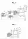
FIG. 2 is a circuit diagram showing a configuration of a conventional foldback overcurrent protection circuit corresponding to a voltage regulator constituted by a depletion transistor as an output transistor. When output current flows through the depletion output transistor 4, detection current also flows through a foldback overcurrent protection circuit 8 accordingly.
When a level of the detection current reaches a predetermined value which is set inside the foldback overcurrent protection circuit 8, the foldback overcurrent protection circuit 8 starts to control the output current flowing through the depletion output transistor 4. In this case, source voltage becomes output voltage since the depletion output transistor 4 operates as a source follower. In order that the output current vs. output voltage characteristic curve should show a foldback characteristic, gate voltage of the depletion output transistor 4 must be lower than the output voltage. In addition, when the output voltage is at the GND level, in order to further reduce the output current, the gate voltage needs to be made negative. However, in the conventional foldback overcurrent protection circuit, it is difficult to reduce the output current flowing through the depletion output transistor since the output transistor is controlled by a circuit which operates at the input voltage VDD and whose reference voltage is GND by using a detection voltage within the output voltage ranging between input voltage VDD and GND.
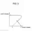
The solid line in FIG. 3 shows the output current vs. output voltage characteristic in overcurrent detection state by the foldback overcurrent protection circuit corresponding to the voltage regulator constituted by a depletion output transistor. The dotted line shows a curve which is required for a foldback protection circuit and which has already been implemented in a regulator constituted by an enhancement mode output transistor. As shown in the figure, the output current increases from a point “v” on a characteristic curve before detection of overcurrent and at the knee point overcurrent is detected. When overcurrent is detected, the output current decreases. Through a point “b”, however, the output current increases to a point “c” on the characteristic curve, not to a point “a”. Thus, the output current is not reduced, but increases (refer to JP 7-74976 B for example).
Heretofore, the foldback overcurrent protection circuit for the voltage regulator constituted by a depletion mode output transistor has a disadvantage in that it is difficult to control the output current vs. output voltage characteristic to show an ideal foldback characteristic because the output voltage ranging between VDD and GND is utilized for the detection voltage for the overcurrent protection circuit.
SUMMARY OF THE INVENTIONIn the light of the foregoing, the present invention has been made in order to solve the above-mentioned problems associated with the prior art, and it is, therefore, an object of the present invention to provide a regulator constituted by a depletion mode output transistor having an overcurrent protection circuit which is capable of controlling the output current vs. output voltage characteristic to show a foldback characteristic curve by operating a negative voltage generating circuit upon detection of an overcurrent.
In order to attain the above-mentioned object, the present invention provides a voltage regulator constituted by a depletion mode output transistor with an overcurrent protection circuit, including: a foldback overcurrent protection circuit, an output voltage detection resistor, a first logic generating circuit which receives an overcurrent detection signal from the foldback overcurrent protection circuit as its input, a second logic generating circuit which receives a detection signal from the output voltage detection resistor representing decrease of the output voltage as its input, a negative voltage generating circuit, and an AND circuit.
BRIEF DESCRIPTION OF THE DRAWINGSIn the accompanying drawings:
FIG. 1 is a circuit diagram showing a configuration of an overcurrent protection circuit according to an embodiment of the present invention;
FIG. 2 is a circuit diagram showing a configuration of a conventional overcurrent protection circuit; and
FIG. 3 is a graph showing output current vs. output voltage characteristic at detection of overcurrent with the overcurrent protection circuit of the embodiment of the present invention (dot line in part) and the conventional output current vs. output voltage characteristics at detection of overcurrent with the conventional overcurrent protection circuit (solid line).
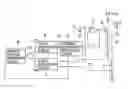
DETAILED DESCRIPTION OF THE PREFERRED EMBODIMENTSA preferred embodiment of an overcurrent protection circuit of the present invention will hereinafter be described in detail with reference to the accompanying drawings. FIG. 1 is a circuit diagram showing a configuration of an overcurrent protection circuit according to an embodiment of the present invention. A voltage regulator constituted by a depletion mode output transistor includes a reference voltage source 1, an amplifier 2, a feedback resistor 3, and a depletion mode output transistor 4. In addition, an overcurrent protection circuit for carrying out control so as to obtain the foldback output current vs. output voltage characteristic includes an output voltage detection resistor 5, a first logic generating circuit 6 which receives an overcurrent detection signal 11 as its input, a second logic generating circuit 7 which receives a detection signal 13 representing decrease of the output voltage as its input, a foldback overcurrent protection circuit 8, a negative voltage generating circuit 9, and an AND circuit 10.
First of all, an operation of the overcurrent protection circuit of this embodiment will hereinafter be described with reference to FIG. 1. When an output current flows through the depletion mode output transistor 4, detection current flows through the foldback overcurrent protection circuit 8 accordingly. When a level of the detection current reaches a predetermined value which is set inside the foldback overcurrent protection circuit 8, the foldback overcurrent protection circuit 8 operates to start the control for the output current flowing through the depletion mode output transistor 4. In addition, the detection signal 11 is also sent from the foldback overcurrent protection circuit 8. After start of the control for the output current, transient current is not needed to be detected, but a constantly flowing overcurrent has to be detected from the output current flowing through the depletion mode output transistor 4, so the first logic generating circuit 6 generates an overcurrent delay signal 12 by giving a predetermined delay time to the detection signal 11.
At the same time, when the output voltage lowers to a voltage which is determined by the reference voltage source 1 and the output voltage detection resistor 5 by controlling the output current, the second logic generating circuit 7 generates a voltage detection signal 14 based on the resistor voltage division output signal 13 of the output voltage detection resistor 5 and the reference voltage source 1. The AND circuit 10 processes the two signals, the overcurrent delay signal 12 and the voltage detection signal 14, thereby operating the negative voltage generating circuit 9, a negative voltage output from the negative voltage generating circuit 9 controls the gate of the depletion mode output transistor 4 through the foldback overcurrent protection circuit 8. That is, in a case where the output voltage is reduced when the constant overcurrent flows through the depletion mode output transistor 4 right after the overcurrent is detected, the control conforming to the foldback output current vs. output voltage characteristic is carried out. FIG. 3 shows the output current vs. output voltage characteristic in this case. As apparent from FIG. 3, a point on the characteristic curve corresponding to the output current starts from the point “v” before detection of the overcurrent to pass through the point “b” at which the negative voltage output after detection of the overcurrent controls the gate of the depletion mode output transistor 4 and then follows a locus indicated by a dotted line to reach a final point “a”. Thus, the foldback output current vs. output voltage characteristic is obtained.
Claims
1. An overcurrent protection circuit for a voltage regulator constituted by a depletion mode output transistor, comprising:
an output voltage detection resistor;
a first logic generating circuit which receives an overcurrent detection signal as its input;
a second logic generating circuit which receives a detection signal representing decrease of the output voltage as its input;
a foldback overcurrent protection circuit which sends the overcurrent detection signal to the first logic generating circuit;
an AND circuit whose input signals are an overcurrent delay signal generated by the first logic generating circuit and a voltage detection signal generated by the second logic generating circuit; and
a negative voltage generating circuit which provides negative voltage to the depletion mode output transistor.
Images & Drawings included:
Sources:
- United States Patent and Trademark Office - verify current appl. status at the USPTO↗
Similar patent applications:
- » 20220416531
Overcurrent protection circuit, overcurrent protection method, clock signal generation circuit and display device - » 20200067300
Overcurrent protection circuit, overcurrent protection method, and display device - » 20230308088
Overcurrent protection circuit for protecting semiconductor device from overcurrent at high speed, and switching circuit provided with the overcurrent protection circuit - » 20240213930
OVERCURRENT PROTECTION CIRCUIT AND POWER AMPLIFIER INCLUDING OVERCURRENT PROTECTION CIRCUIT - » 20120044602
REGULATING SYSTEM HAVING OVERVOLTAGE PROTECTION CIRCUIT AND OVERCURRENT PROTECTION CIRCUIT - » 20110291634
Overcurrent protection circuit and overcurrent protection method - » 20090201618
Power supply circuit, overcurrent protection circuit for the same, and electronic device - » 20230065691
CHARGING/DISCHARGING OVERCURRENT PROTECTION CIRCUIT AND OVERCURRENT PROTECTION METHOD THEREFOR - » 20230393599
CURRENT DETECTION CIRCUIT, OVERCURRENT PROTECTION CIRCUIT, AND LINEAR POWER SUPPLY - » 20240213976
High Side Current Detection Circuit, Overcurrent Protection Circuit, Calibration Method and Electronic Devices
Recent applications in this class:
- » 20250085731 2025-03-13
CONSTANT VOLTAGE GENERATOR CIRCUIT OPERATING AT LOW VOLTAGE POTENTIAL DIFFERENCE BETWEEN INPUT VOLTAGE AND OUTPUT VOLTAGE - » 20240231401 2024-07-11
Constant voltage generator circuit operating at low voltage potential difference between input voltage and output voltage - » 20240012437 2024-01-11
CURRENT LIMITER, METHOD OF OPERATING THE SAME, AND HOTSWAP MODULE - » 20230251678 2023-08-10
Methods and apparatuses for extended current limit for power regulation - » 20230130733 2023-04-27
Low dropout linear regulator and control circuit thereof - » 20210294369 2021-09-23
Methods and apparatuses for extended current limit for power regulation - » 20200012304 2020-01-09
Temperature dependent current limit control for fast-charging and safe operating area (SOA) protection - » 20180373282 2018-12-27
Automatically restarting a voltage foldback circuit - » 20180120884 2018-05-03
Variable ratio charge pump with peak current and average current limiting circuitry - » 20120229109 2012-09-13
Lambda correction for current foldback
Recent applications for this Assignee:
- » 20190264742 2019-08-29
Method of manufacturing an enveloping layer-coated slide bearing - » 20190025766 2019-01-24
Timepiece, timepiece system, and method of controlling timepiece - » 20180306243 2018-10-25
Rolling bearing - » 20180306242 2018-10-25
Structure with thermoplastic elastomer enveloping layer, bearing, and drive module - » 20180306240 2018-10-25
Enveloping layer-coated slide bearing and drive module - » 20180241280 2018-08-23
Vibration generation device and electronic device - » 20180203417 2018-07-19
Timepiece - » 20180097302 2018-04-05
Portable printer - » 20170331349 2017-11-16
Vibration generation device and electronic apparatus - » 20170315509 2017-11-02
Mechanical component, mechanical component manufacturing method, movement, and timepiece