Package of a semiconductor device with a flexible wiring substrate and method for the same
US20050161815A1
2005-07-28
10/764,469
2004-01-27
Abstract:
A package of a semiconductor device with a flexible wiring substrate and a method thereof are provided. The package of the semiconductor device includes a semiconductor substrate with at least one pad on a surface thereof, a bump bonded to the pad, an adhesive layer on the bump, and a flexible wiring substrate having at least one contact section being electrically connected with the bump by the adhesive layer. The present invention makes the flexible wiring substrate directly conductively attached onto the semiconductor substrate. The package size is shrunk and the cost down can be obtained.
Inventors:
- Joseph Sun 4 🇹🇼 Hsin-Chu City, Taiwan
- Kuang-Chih Cheng 4 🇹🇼 Yun-Lin, Taiwan
- Ming-Chieh Chen 4 🇹🇼 Hsin-Chu City, Taiwan
Interested in similar patents?
Get notified when new applications in this technology area are published.
Classification:
H01L27/14618 » CPC main
Devices consisting of a plurality of semiconductor or other solid-state components formed in or on a common substrate including semiconductor components sensitive to infra-red radiation, light, electromagnetic radiation of shorter wavelength or corpuscular radiation and specially adapted either for the conversion of the energy of such radiation into electrical energy or for the control of electrical energy by such radiation; Devices controlled by radiation; Imager structures; Structural or functional details thereof Containers
H01L23/49816 » CPC further
Details of semiconductor or other solid state devices; Arrangements for conducting electric current to or from the solid state body in operation, e.g. leads, terminal arrangements ; Selection of materials therefor consisting of soldered constructions; Leads, on insulating substrates,; Additional leads joined to the metallisation on the insulating substrate, e.g. pins, bumps, wires, flat leads Spherical bumps on the substrate for external connection, e.g. ball grid arrays [BGA]
H01L23/4985 » CPC further
Details of semiconductor or other solid state devices; Arrangements for conducting electric current to or from the solid state body in operation, e.g. leads, terminal arrangements ; Selection of materials therefor consisting of soldered constructions; Leads, on insulating substrates, Flexible insulating substrates
H05K3/361 » CPC further
Apparatus or processes for manufacturing printed circuits; Assembling printed circuits with other printed circuits Assembling flexible printed circuits with other printed circuits
H05K3/361 » CPC further
Apparatus or processes for manufacturing printed circuits; Assembling printed circuits with other printed circuits Assembling flexible printed circuits with other printed circuits
H05K3/323 » CPC further
Apparatus or processes for manufacturing printed circuits; Assembling printed circuits with electric components, e.g. with resistor electrically connecting electric components or wires to printed circuits by conductive adhesives by applying an anisotropic conductive adhesive layer over an array of pads
H05K2201/0367 » CPC further
Indexing scheme relating to printed circuits covered by; Conductive materials; Structure of the conductor; Conductor shape Metallic bump or raised conductor not used as solder bump
H05K2201/0367 » CPC further
Indexing scheme relating to printed circuits covered by; Conductive materials; Structure of the conductor; Conductor shape Metallic bump or raised conductor not used as solder bump
H01L2924/00014 » CPC further
Indexing scheme for arrangements or methods for connecting or disconnecting semiconductor or solid-state bodies as covered by; Technical content checked by a classifier the subject-matter covered by the group, the symbol of which is combined with the symbol of this group, being disclosed without further technical details
H01L2924/00 » CPC further
Indexing scheme for arrangements or methods for connecting or disconnecting semiconductor or solid-state bodies as covered by
Description
BACKGROUND OF THE INVENTION1. Field of the Invention
The present invention relates to a package of a semiconductor device, and more particularly to a package of a semiconductor device electrically connected with a flexible printed circuit board.
2. Description of the Prior Art
Ever increasing industry demand for smaller and smaller electronic packages with low profile, higher area density and increasing number of input/output connections (I/Os) has led to increasing demand for the chip scale package. Use of such packages may be found in small portable products, such as cellular phones, pagers, and the like. Moreover, a flexible printed circuit board (FPC) is widely used in view of the freedom of packaging form and the space saving. A wire bonding is frequently used when a high-density package is required or a package space is limited.
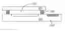
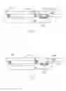
FIG. 1 is a schematic configuration of a known package of an image sensor device incorporated with a handset. The package of the image sensor device has a silicon substrate 101 having at least one pad 105 on a surface thereof and an image sensor device 102, such as CMOS (Complementary Metal-Oxide-Semiconductor) sensor, LCOS (Liquid Crystal-On-Silicon), on the surface. A glass plate 103 is placed above the surface of the silicon substrate 101 having the image sensor device 102. The glass plate 103 is used for preventing the airborn dust or other particles adhered unto the image sensor device 102, causing the image sensor device 102 damage. The glass plate 103 is attached unto the silicon substrate 101 by adhesive material 104. The silicon substrate 101 is placed on a printed circuit board 100, and the pad 105 is connected with an I/O terminal of the printed circuit board 100 via a metal wire 106 by wire bonding. A lens housing 107 enclosing the whole silicon substrate 101 is held on the printed circuit board 100. A lens set 108 is positioned above the glass plate 103 and held by the lens housing 107. A flexible printed circuit board 109 is attached onto the printed circuit board 100. In general, the fingers of the leads of the flexible printed circuit board 109 are bonded to a contact portion of the printed circuit board 100. The flexible printed circuit board 109 is electrically connected to a main board of the handset. The image sensor device 102 captures image signals, and transfers the image signals to electric signals. Then, the electric signals are transmitted to the flexible printed circuit board 109 via an interface, i.e., the printed circuit board 100, and then transmitted to the main board of the handset.
The package of the image sensor device of FIG. 1 is troublesome and bulky. However, the flexible printed circuit board 109 cannot be directly attached unto the silicon substrate 101 due to the configuration of the image sensor device. It is necessary to form a gold bump on the pad 105 of the silicon substrate 101 before the fingers of the leads of the flexible printed circuit board 109 are to be electrically connected with the pad 105. However, the gold bump cannot be electroplated on the pad 105 of the silicon substrate 101 because the glass plate 103 has been covered on the silicon substrate 101. When the silicon substrate 101 is uncovered with the glass plate 103, the image sensor device 102 is easily subjected to damage by the particles during the process of the package, and resulting in a low yield. Therefore, the flexible printed circuit board 109 cannot be directly attached unto the silicon substrate 101 in view of the configuration of the package of the image sensor device.
Accordingly, it is an intention to provide a package method of a semiconductor device, which can overcome the drawbacks of the prior art.
SUMMARY OF THE INVENTIONIt is one objective of the present invention to provide a package of a semiconductor device with a flexible wiring substrate, which directly attaches a flexible printed circuit board unto a semiconductor substrate, so that the package size can be reduced and the cost down can be obtained.
It is another objective of the present invention to provide a package of a semiconductor device with a flexible wiring substrate, which is suitable to a package of an image sensor device.
In order to achieve the above objectives of this invention, the present invention provides a package of a semiconductor device with a flexible wiring substrate and a method thereof. The package of the semiconductor device of the present invention includes a semiconductor substrate with at least one pad on a surface thereof, a bump bonded to the pad, an adhesive layer on the bump, and a flexible wiring substrate having at least one contact section being electrically connected with the bump by the adhesive layer.
The present invention makes the flexible wiring substrate directly electrically connected with the semiconductor device. The shrinkage of the package of the semiconductor device becomes realizable. Moreover, the package method of the present invention is simple and easily completed.
BRIEF DESCRIPTION OF THE DRAWINGSThe objectives and features of the present invention as well as advantages thereof will become apparent from the following detailed description, considered in conjunction with the accompanying drawings.
FIG. 1 is a schematic configuration of a known package of an image sensor device incorporated with a handset;
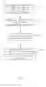
FIG. 2 through FIG. 6 is various schematic cross-sectional views respectively corresponding to one stage of a package method of the present invention according to an embodiment; and
FIG. 7 is a process flow of the package method of the present invention corresponding to FIG. 2 through FIG. 6.
DESCRIPTION OF THE EMBODIMENTSThe present invention provides a package of a semiconductor device electrically connected with a flexible wiring substrate and a method thereof. The package method of a semiconductor device provided by the present invention is suitable to an application for a wafer covered with a transparent plate.
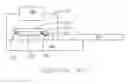
The package of a semiconductor device provided by the present invention and the method thereof will be described in detail in accordance with an embodiment of the present invention accompanying with drawings. FIG. 7 is a process flow of the package method of the present invention in accordance with the embodiment, and FIG. 2 through FIG. 6 is various schematic cross-sectional views, respectively corresponding to each step of the process flow of FIG. 7. Referring to FIG. 7, in step 70, a transparent plate 201 is covered on a surface of a wafer 200 having a plurality of image sensor device 203 and a plurality of pad 204 formed thereon, as shown in FIG. 2. The pad 204 can be an aluminum pad or a copper pad. The image sensor device 203 can be a kind of light-receiving element, such as CMOS sensor, LCOS and the like, and the transparent plate 201 can be a lens or a glass plate. The transparent plate 201 is held on the wafer 200 by adhesive material 202 and used for protecting the image sensor devices 203 from being damaged by particles adhered thereto. The wafer 200 covered with the transparent plate 201 is subjected to a dicing process and divided into chips, also known as “dies”. The dicing process may be accomplished by several means, including a chemical method using acetic acid or fluoroacetic acid, and a scribing method using a diamond cutter. As a consequence, a die 200 having at least one pad 204 on a surface thereof is provided, as shown in FIG. 3. The die 200 will be called “semiconductor substrate” hereinafter. Then, in step 72, a bump is formed on the pad 204 of the semiconductor substrate 200. The bump can be a gold stud bump 205 being formed by a process as the following: a torch rod is placed close a tip of an gold wire, between which a high voltage is applied to generate a spark discharge therebetween, thereby providing a ball at the tip of the gold wire by heat. The ball is then pressed on the pad 204 of the semiconductor substrate 200 by using a bonding tool (capillary), the gold wire being pulled up thereby to provide the gold stud bump 205 on the pad 204, as shown in FIG. 4.
Following, in step 74, an anisotropic conductive paste 206 is applied on the gold stud bump 205 as an adhesive layer, as shown in FIG. 5. The anisotropic conductive paste 206 can be an epoxy-based adhesive resin paste with conductive fillers 207, such as metallic particles, therein. Then, in step 76, a flexible wiring substrate 209, for example, a flexible printed circuit board, having at least one contact section, is provided. The contact section of the flexible wiring substrate 209 is attached unto the anisotropic conductive paste 206 on the gold stud bump 205 to compress the anistropic conductive paste 206 trapped in the interface between the gold stud bump 205 and the contact section of the flexible wiring substrate 209. When the anisptropic conductive paste 206 is compressed, the conductive fillers 207 inside the interface will align themselves and create a conductive path between the semiconductor substrate 200 and the flexible wiring substrate 209. In other words, electrical interconnection between the gold stud bump 205 and the contact section of the flexible wiring substrate 209 is made by conductive fillers' 207 mechanical contact therebetween.
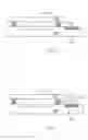
Alternately, as shown in FIG. 6, a non-conductive paste 208 can be applied on the gold stud bump 205 instead of the anisotropic conductive paste 206. The non-conductive paste 208 can be an epoxy adhesive resin. Then, the contact section of the flexible wiring substrate 200 is attached unto the non-conductive paste 208 on the gold stud bump 205 to compress the non-conductive paste 208 trapped in the interface between the gold stud bump 205 and the contact section of the flexible wiring substrate 209. Then, the non-conductive paste 206 trapped in the interface is squeezed out from the interface, and around the gold stud bump 205 and the contact section of the flexible wiring substrate 209. As a consequence, the contact section of the flexible wiring substrate 209 directly contacts with the gold stud bump 205, and both of them are attached together by the non-conductive paste 208 around them.
The present invention makes the flexible wiring substrate 209 directly electrically connected with the semiconductor substrate 200. The shrinkage of the package of the semiconductor device becomes realizable. The package method of the present invention is simple and easily completed. It is possible to attain a purpose of cost down by the present invention.
The embodiments are only used to illustrate the present invention, not intended to limit the scope thereof. Many modifications of the embodiments can be made without departing from the spirit of the present invention.
Claims
1. A package of a semiconductor device with a flexible wiring substrate, comprising:
a semiconductor substrate with at least one pad on a surface thereof;
a bump bonded to said pad;
an adhesive layer on said bump; and
a flexible wiring substrate having at least one contact section being electrically connected with said bump by said adhesive layer.
2. The package of claim 1, wherein said bump is stud bump.
3. The package of claim 2, wherein said bump is gold stud bump.
4. The package of claim 1, wherein said adhesive layer includes non-conductive paste.
5. The package of claim 2, wherein said adhesive layer includes non-conductive paste.
6. The package of claim 1, wherein said adhesive layer includes anistropic conductive paste.
7. The package of claim 2, wherein said adhesive layer includes anistropic conductive paste.
8. The package of claim 1, wherein said semiconductor substrate having image sensors on the surface thereof having said pad.
9. The package of claim 8, wherein a transparent plate covered on the surface of said semiconductor substrate having said image sensors.
10. The package of claim 9, wherein said bump is stud bump.
11. The package of claim 10, wherein said adhesive layer includes anistropic conductive paste.
12. The package of claim 10, wherein said adhesive layer includes non-conductive paste.
13. A package method of a semiconductor device with a flexible wiring substrate, comprising:
providing a semiconductor substrate having at least one pad on a surface thereof;
forming a bump on said pad of said semiconductor substrate;
forming an adhesive layer on said bump; and
attaching a flexible wiring substrate unto said semiconductor substrate, wherein said flexible wiring substrate is provided with at least one contact section, and said contact section is electrically connected with said pad by said adhesive layer.
14. The package method of claim 13, wherein said bump is formed by a stud bump process.
15. The package method of claim 14, wherein said bump is formed by a gold stud bump process.
16. The package method of claim 13, wherein said adhesive layer includes non-conductive paste.
17. The package method of claim 14, wherein said adhesive layer includes non-conductive paste.
18. The package method of claim 13, wherein said adhesive layer includes anistropic conductive paste.
19. The package method of claim 14, wherein said adhesive layer includes anistropic conductive paste.
20. The package method of claim 16, wherein said adhesive layer includes epoxy-based non-conductive paste.
Images & Drawings included:
Sources:
- United States Patent and Trademark Office - verify current appl. status at the USPTO↗
Similar patent applications:
- » 20050161756
Package of a semiconductor device with a flexible wiring substrate and method for the same - » 20060113654
Package of a semiconductor device with a flexible wiring substrate and method for the same - » 20060202333
Package of a semiconductor device with a flexible wiring substrate and method for the same
Recent applications in this class:
- » 20250048762 2025-02-06
SEMICONDUCTOR DEVICE, ELECTRONIC APPARATUS, AND MANUFACTURING METHOD OF SEMICONDUCTOR DEVICE - » 20250048761 2025-02-06
SEMICONDUCTOR PACKAGE STRUCTURE AND METHOD FOR PRODUCING THE SAME - » 20250048760 2025-02-06
ELECTRONIC DEVICE - » 20250040276 2025-01-30
IMAGE SENSOR PACKAGE - » 20250040275 2025-01-30
SENSOR PACKAGE STRUCTURE AND SENSING MODULE THEREOF - » 20250031468 2025-01-23
METHOD OF MANUFACTURING CONNECTION STRUCTURE, CONNECTION STRUCTURE, FILM STRUCTURE, AND METHOD OF MANUFACTURING FILM STRUCTURE - » 20250015105 2025-01-09
SUBSTRATE LAMINATE, IMAGE SENSOR, AND METHOD FOR MANUFACTURING SUSTRATE LAMINATE - » 20250006756 2025-01-02
IMAGE SENSING MODULE MANUFACTURING METHOD - » 20250006755 2025-01-02
SEMICONDUCTOR DEVICE AND ELECTRONIC EQUIPMENT - » 20240429253 2024-12-26
SEMICONDUCTOR APPARATUS AND ELECTRONIC DEVICE