Conducting structure of a multi-layers IC board
US20050183885A1
2005-08-25
10/780,653
2004-02-19
Abstract:
The invention relates to a conducting structure of a multi-layers IC board, which includes conducting rod being received in aperture of the IC board to obtain an effective connection and conduction. And the conducting wire is placed horizontally on the IC board, which has its ending pin and annular metal ring to contact with two apertures respectively and to be welded thereon for perfect conduction and smaller assembled volume.
Interested in similar patents?
Get notified when new applications in this technology area are published.
Classification:
H05K1/0243 » CPC main
Printed circuits; Details; Electrical arrangements not otherwise provided for; High frequency adaptations Printed circuits associated with mounted high frequency components
H05K1/0243 » CPC main
Printed circuits; Details; Electrical arrangements not otherwise provided for; High frequency adaptations Printed circuits associated with mounted high frequency components
H01R9/0515 » CPC further
Structural associations of a plurality of mutually-insulated electrical connecting elements, e.g. terminal strips or terminal blocks; Terminals or binding posts mounted upon a base or in a case; Bases therefor; Connectors arranged to contact a plurality of the conductors of a multiconductor cable, e.g. tapping connections for coaxial cables Connection to a rigid planar substrate, e.g. printed circuit board
H05K3/4046 » CPC further
Apparatus or processes for manufacturing printed circuits; Forming printed elements for providing electric connections to or between printed circuits; Through-connections; Vertical interconnect access [VIA] connections using auxiliary conductive elements, e.g. metallic spheres, eyelets, pieces of wire
H01R4/023 » CPC further
Electrically-conductive connections between two or more conductive members in direct contact, i.e. touching one another; Means for effecting or maintaining such contact; Electrically-conductive connections having two or more spaced connecting locations for conductors and using contact members penetrating insulation; Soldered or welded connections between cables or wires and terminals
H01R12/523 » CPC further
Structural associations of a plurality of mutually-insulated electrical connecting elements, specially adapted for printed circuits, e.g. printed circuit boards [PCBs], flat or ribbon cables, or like generally planar structures, e.g. terminal strips, terminal blocks; Coupling devices specially adapted for printed circuits, flat or ribbon cables, or like generally planar structures; Terminals specially adapted for contact with, or insertion into, printed circuits, flat or ribbon cables, or like generally planar structures; Fixed connections for rigid printed circuits or like structures connecting to other rigid printed circuits or like structures by an interconnection through aligned holes in the boards or multilayer board
H05K1/0298 » CPC further
Printed circuits; Details; Conductive pattern lay-out details not covered by sub groups - Multilayer circuits
H05K1/0298 » CPC further
Printed circuits; Details; Conductive pattern lay-out details not covered by sub groups - Multilayer circuits
H05K3/328 » CPC further
Apparatus or processes for manufacturing printed circuits; Assembling printed circuits with electric components, e.g. with resistor electrically connecting electric components or wires to printed circuits by welding
H05K3/328 » CPC further
Apparatus or processes for manufacturing printed circuits; Assembling printed circuits with electric components, e.g. with resistor electrically connecting electric components or wires to printed circuits by welding
H05K3/3405 » CPC further
Apparatus or processes for manufacturing printed circuits; Assembling printed circuits with electric components, e.g. with resistor electrically connecting electric components or wires to printed circuits by soldering Edge mounted components, e.g. terminals
H05K3/3405 » CPC further
Apparatus or processes for manufacturing printed circuits; Assembling printed circuits with electric components, e.g. with resistor electrically connecting electric components or wires to printed circuits by soldering Edge mounted components, e.g. terminals
H05K2201/09809 » CPC further
Indexing scheme relating to printed circuits covered by; Shape and layout; Shape and layout details of conductors covering at least two types of conductors provided for in - Coaxial layout
H05K2201/09809 » CPC further
Indexing scheme relating to printed circuits covered by; Shape and layout; Shape and layout details of conductors covering at least two types of conductors provided for in - Coaxial layout
H05K2201/10356 » CPC further
Indexing scheme relating to printed circuits covered by; Details of components or other objects attached to or integrated in a printed circuit board; Other objects, e.g. metallic pieces Cables
H05K2201/10356 » CPC further
Indexing scheme relating to printed circuits covered by; Details of components or other objects attached to or integrated in a printed circuit board; Other objects, e.g. metallic pieces Cables
H05K2201/10401 » CPC further
Indexing scheme relating to printed circuits covered by; Details of components or other objects attached to or integrated in a printed circuit board; Other objects, e.g. metallic pieces Eyelets, i.e. rings inserted into a hole through a circuit board
H05K2201/10401 » CPC further
Indexing scheme relating to printed circuits covered by; Details of components or other objects attached to or integrated in a printed circuit board; Other objects, e.g. metallic pieces Eyelets, i.e. rings inserted into a hole through a circuit board
Description
FIELD OF THE INVENTIONThe present invention relates to an improvement of a conducting structure of a multi-layers IC board, which can conduct each layer of IC board effectively and decreases the combined volume of the assembly.
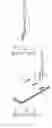
BACKGROUND OF THE INVENTIONIt is known that many new invention of technology is designed to be lighter and smaller for easy carriage and use. Hence, multi-layers IC board has been developed for application. It is known that a conducting wire (1) is used to conduct every layers of the IC board (2), as shown in FIG. 1 to 4. The conducting wire (1) has its annular metal ring (12) to connect with an extended pin (13). The extended pin (13) and the ending pin (11) of the wire (1) are inserted into two neighborhood apertures (21) of the multi-layers IC board (2) and are welded for firm connection and conduction. But by the said method of connection between the pins and the IC board, the welding can not completely filled the whole aperture (21) that remains space therein, as shown in FIG. 2. So the conducting effect is not good. Moreover, the conducting wire (1) is perpendicular to the IC board (2) that occupies a large volume even the wire (1) is bent as in FIG. 4.
SUMMARY OF THE INVENTIONThe present invention is to provide a conducting structure of a multi-layers IC board to overcome the drawback of the prior art and to decrease the assembled volume of the wire and the IC board. Now, accompanying with the following drawings, the character of the present invention will be described here and after.
BRIEF DESCRIPTION OF THE DRAWINGSFIG. 1 is an exploded perspective view showing a conventional conducting wire and a multi-layers IC board.
FIG. 2 is an assembled perspective view of FIG. 1.
FIG. 3 is a perspective view of FIG. 2 after being welded.
FIG. 4 is across-sectional plan view of FIG. 3.
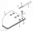
FIG. 5 is an exploded perspective view showing a conducting wire and a multi-layers IC board according to the present invention.
FIG. 6 is an assembled perspective view of FIG. 5.
FIG. 7 is a perspective view of FIG. 6 after being welded.
FIG. 8 is across-sectional plan view of FIG. 7.
DETAILED DESCRIPTION OF THE PREFERRED EMBODIMENTReferring to FIG. 5 to 8, the present invention includes a conducting rod (3), which is received in an aperture (21) of a multi-layers IC board (2). Hence, the conducting rod (3) can contact with each layer of the IC board effectively to provide certain conducting purpose therebetween. Each aperture (21) is provided with a conducting rod (3).
The conducting wire (1) is placed on the IC board (2) horizontally that makes its ending pin (11) and annular metal ring (13) contact with two neighborhood conducting rods (3) respectively. Then the wire (1) can be welded on the board (2) to obtain a firm connection.
Accordingly, the rod (3) is effectively conductive with each layer of the IC board (2) and the pin (11) and the metal ring (13) are capable of being connected with the rod (3) in secure. It is found that the conduction provided by the present invention will be better than the prior art. Furthermore, the conducting wire (1) is placed on the IC board (2) directly that occupies a smaller volume for effective application and improvement.
Claims
1. A conducting structure of a multi-layers IC board including a conducting wire and a conducting rod being received in each aperture of the IC board, wherein the rod is conducted with each layer of the IC board, and the conducting wire being placed on the board to have its ending pin and annular metal ring contact with two neighborhood apertures and be welded together for effective conduction.
Images & Drawings included:


Sources:
- United States Patent and Trademark Office - verify current appl. status at the USPTO↗
Recent applications in this class:
- » 20250142714 2025-05-01
MULTI-CONFIGURABLE ANTENNA TUNER CIRCUIT BOARD - » 20250120007 2025-04-10
RECEPTACLE ASSEMBLY AND CIRCUIT BOARD - » 20250071885 2025-02-27
RADIO FREQUENCY FRONT-END STRUCTURES - » 20250071884 2025-02-27
ADDITIVE MANUFACTURED COAX-LIKE CONNECTION FOR MICROSTRIP ANTENNA FEEDING AND SIGNAL INTEGRITY IN HIGH FREQUENCY PCB - » 20250063652 2025-02-20
PRINTED CIRCUIT BOARD (PCB) MODULE COMPRISING AN EMBEDDED RADIO-FREQUENCY SEMICONDUCTOR DIE - » 20250048538 2025-02-06
INSERTABLE WIRELESS COMMUNICATION DEVICE FOR A POWER TOOL - » 20250048537 2025-02-06
LOW SWITCHING LOSS INVERTER CIRCUIT BOARD - » 20250040032 2025-01-30
CIRCUIT BOARD - » 20240389222 2024-11-21
RADIO FREQUENCY MODULE, COMMUNICATION DEVICE, AND FILTER - » 20240365465 2024-10-31
HIGH FREQUENCY MODULE AND COMMUNICATION DEVICE