Plasma processing apparatus and method of designing the same
US20050194097A1
2005-09-08
11/064,975
2005-02-25
Abstract:
Disclosed is a plasma processing apparatus having a plasma producing portion and a porous plate provided between the plasma producing portion and an object to be processed, wherein the porous plate has a plurality of holes which are made non-uniform with respect to at least one of shape, size and disposition. Specifically, the shape, the size or the disposition of the holes is determined on the basis of an active species distribution at the plasma producing portion and of diffusion calculation, so that plasma active species adjacent the object to be processed has desired concentration and distribution. This assures uniform plasma distribution adjacent the object while a decrease of plasma density can be well suppressed.
Assignee:
- CANON KABUSHIKI KAISHA 58,598 🇯🇵 Tokyo, Japan
Interested in similar patents?
Get notified when new applications in this technology area are published.
Classification:
H01L21/67069 » CPC main
Processes or apparatus adapted for the manufacture or treatment of semiconductor or solid state devices or of parts thereof; Apparatus specially adapted for handling semiconductor or electric solid state devices during manufacture or treatment thereof; Apparatus specially adapted for handling wafers during manufacture or treatment of semiconductor or electric solid state devices or components ; Apparatus not specifically provided for elsewhere; Apparatus not specifically provided for elsewhere; Apparatus for manufacture or treatment; Apparatus for fluid treatment for etching for drying etching
H01J37/32357 » CPC further
Discharge tubes with provision for introducing objects or material to be exposed to the discharge, e.g. for the purpose of examination or processing thereof; Gas-filled discharge tubes; Arrangements for generation of plasma specially adapted for examination or treatment of objects, e.g. plasma sources Generation remote from the workpiece, e.g. down-stream
H01J37/32422 » CPC further
Discharge tubes with provision for introducing objects or material to be exposed to the discharge, e.g. for the purpose of examination or processing thereof; Gas-filled discharge tubes; Arrangements for generation of plasma specially adapted for examination or treatment of objects, e.g. plasma sources Arrangement for selecting ions or species in the plasma
Description
FIELD OF THE INVENTION AND RELATED ARTThis invention relates generally to a plasma processing apparatus such as, for example, an etching apparatus, a nitriding apparatus or an oxidation apparatus, for example, to be used in a semiconductor manufacturing process for semiconductor substrate or liquid crystal substrate, for example. More particularly, the invention concerns a plasma processing apparatus by which the amount of plasma active species or active molecules adjacent a substrate (object to be processed) can be made into desired density (or concentration) and distribution.
For improved yield of chips to be produced on a semiconductor substrate, the process uniformity over the semiconductor substrate surface is very important in plasma processing apparatuses. In order to accomplish the process uniformity over the semiconductor substrate surface, many attempts have been made in plasma processing apparatuses. Use of a porous plate is an example.
As an example, Japanese Laid-Open Patent Application, Publication No. 2000-58294 shows a CVD (chemical vapor deposition) apparatus wherein, for assuring deposition of a thin film upon a semiconductor substrate with uniform thickness, the thickness of a porous plate is changed to control the amount of reaction gas supply to individual points on the semiconductor substrate surface. The apparatus of this prior art example is a CVD apparatus wherein a semiconductor substrate is processed with relatively high pressure, and the structure is arranged to perform air flow control in a viscous flow pressure region. In order to provide a large pressure difference between the top and bottom of the porous plate and to make the gas flow rates through the holes even, a large number of holes having very small diameter Φ=0.1 to 1 mm are formed in the porous plate. The thickness distribution of the porous plate is determined on the basis of viscous flow relational equation that the gas flow rate through the hole is proportional to the square of the depth, while referring to the results of experiments. Although this prior art example is suitably applicable to a case wherein a thin film is to be uniformely deposited on a semiconductor substrate, it is unsuitable to a case, such as etching, wherein a semiconductor is to be processed with relatively low pressure. This is because of an antinomy between one need that, since the etching process is carried out in a molecular flow pressure region which is relatively low pressure, the thickness difference should be made large for performing the gas flow rate control based on the thickness distribution of the porous plate and another need that the porous plate should be made as thin as possible to enable efficient ion utilization.
Japanese Laid-Open Patent Application, Publication No. 11-350143 shows a porous plate which is applicable to an ethcing apparatus. In this example, a microwave transmission window is provided on a surface to be opposed to a semiconductor substrate, and plasma is produced by the microwave. The microwave transmission window comprises three windows. The uppermost window serves to isolate the atmosphere and the vacuum from each other. The middle and bottom windows are formed with small holes for conductance, and a reaction gas is supplied to a semiconductor substrate surface uniformly. This microwave transmission window having three windows and functioning as a porous plate as well is arranged so that the pressure inside the window is made high and also that the space between them is made narrow, to thereby prevent electric discharge inside the window of three-window structure. This prior art example is based on the concept that the amount of reaction gas supply to individual points on the semiconductor substrate surface is made uniform by means of the microwave transmission window (porous plate) so that uniform plasma is produced at the bottom of the microwave transmission window (porous plate), by which the amount of plasma ion supply to the individual points on the semiconductor substrate surface is made uniform. Furthermore, a slot antenna having a hole is provided to produce uniform plasma at underneath the microwave transmission window, thereby to make the microwave transmission distribution approximately uniform.
However, if the slot antenna is designed to provide approximately uniform microwave transmission distribution, although this enables that uniform microwave plasma is produced at underneath the microwave transmission window in a particular restrited condition, but in other conditions it is difficult to produce uniform microwave plasma there. Presumably, this is because, since the surface wave mode is variable with plasma density, plasma can not be excited stably.
There is a further example as disclosed in Japanese Laid-Open Patent Application, Publication No. 5-345982 wherein a microwave surface interference wave is produced btween slots and microwave plasma is excited stably without causing mode jump. In this prior art example, since diffusion is used in a molecular flow pressure region so as to make uniform the plasma distribution adjacent a semiconductor substrate, there is a tendency that the plasma processing chamber and, in turn, the plasma processing apparatus, become large in size. Hence, it has been attempted to make the plasma processing apparatus smaller in size while uniforming the plasma distribution adjacent the substrate by use of a porous plate. However, although the plasma distribution about the substrate was adjusted uniformly when a porous plate having irregularly distributed small holes of a diameter of few milimeters, for example, the contact area between the plasma and the porous plate was enlarged and the plasma density wad decreased considerably. This caused enlargement of the substrate processing time. On the other hand, relatively large holes were used to decrease the contact area with the plasma to suppress the plasma decrease, but the attribution of each hole became large and huge time and effort were spent by trial and error. Thus, it was impractical.
SUMMARY OF THE INVENTIONIt is accordingly an object of the present invention to provide a plasma processing apparatus by which plasma active species adjacent an object to be processed can be made into desired density (concentration) and distribution.
It is another object of the present invention to provide a plasma processing apparatus having a porous plate which is incorporated therein and which is effective to make uniform a plasma distribution adjacent an object to be processed, while suppresssing plasma density decrease, still very easily without relying on trial and error.
In accordance with an aspect of the present invention, to achieve at least one of the above objects, there is provided a plasma processing apparatus, comprising: a plasma producing portion; and a porous plate provided between said plasma producing portion and an object to be processed, wherein said porous plate has a plurality of holes which are made non-uniform with respect to at least one of shape, size and disposition.
In accordance with another aspect of the present invention, there is provided a plasma processing apparatus, comprising: a plasma producing portion; and a porous plate provided between said plasma producing portion and an object to be processed, wherein said porous plate has a plurality of holes being shaped and disposed as determined on the basis of an active species distribution at said plasma producing portion and of diffusion calculation, so that plasma active species adjacent the object to be processed has desired density and distribution.
In accordance with a further aspect of the present invention, there is provided a method of designing a plasma processing apparatus having a plasma producing portion and a porous plate provided between said plasma producing portion and an object to be processed, comprising: determining a shape and disposition of holes of the porous plate on the basis of active species distribution at the plasma producing portion and of diffusion calculation, so that plasma active species adjacent the object has desired density and distribution.
Briefly, in accordance with the present invention, a porous plate having holes which are non-uniform with respect to shape, size and/or distribution is used, by which various densities and distributions of plasma active species can be provided. Particularly, the shape, size and distribution of the holes may be determined in accordance with the active species distribution at the plasma producing portion and with diffusion calculation. This effectively removes the necessity of huge time and efforts required by the trial and error works, and a porous plate that assures desired plasma active species density and distribution can be accomplished easily and conveniently.
These and other objects, features and advantages of the present invention will become more apparent upon a consideration of the following description of the preferred embodiments of the present invention taken in conjunction with the accompanying drawings.
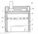
BRIEF DESCRIPTION OF THE DRAWINGSFIG. 1 is a schematic view of a microwave plasma processing apparatus according to a first embodiment of the present invention.
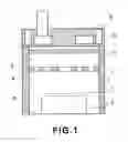
FIG. 2 is a schematic view of a porous plate according to the first embodiment of the present invention.
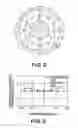
FIG. 3 is a graph for explaining the function and effect of the porous plate according to the first embodiment of the present invention.
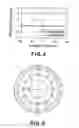
FIG. 4 is a graph for explaining the function and effect of a porous plate according to a second embodiment of the present invention.
FIG. 5 is a schematic view of a porous plate according to a third embodiment of the present invention.
FIG. 6 is a schematic view for explaining disposition of slots in a fourth embodiment of the present invention.
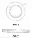
FIG. 7 is a sectional view of a porous plate according to a fifth embodiment of the present invention.
DESCRIPTION OF THE PREFERRED EMBODIMENTSA plasma processing apparatus according to one preferred form of the present invention comprises a plasma processing portion and a porous plate provided between the plasma processing portion and a substrate to be processed, wherein the shape and disposition of holes of the porous plate are determined on the basis of active species density distribution at the plasma producing portion and the diffusion calculation, so as to ensure that the plasma active species adjacent the substrate has uniform distribution. In accordance with this embodiment, the porous plate is designed on the basis of the active species density distribution at the plasma producing portion and of diffusion calculation. Hence, large-diameter holes can be determined without relying on trial and error works, such that a plasma processing apparatus that can provide plasma active species distribution of good uniformity, adjacent the substrate, while suppressing plasma decrease, is accomplished.
Here, the active species density distribution at the plasma producing portion can be detected by use of an electron probe, for example. Further, the diffusion calculation can be done in accordance with equation (1) below, known as ambipolar diffusion equation. It is known that the plasma that arrives at a wall by diffusion is annihilated by recombination quenching at the wall, by an amount as can be represented by equation (2) below. Diffusion coefficient and the like necessary for execution of these equations can be determined on the basis of experiments using an electron probe.
Q=D×ΔN/L×S (1)
In equation (1), Q is the diffusion amount, D is a diffusion coefficient, ΔN is a density difference, L is a length, and S is an area.
Q′=N×C×S (2).
In equation (2), Q′ is the amount of recombination quenching, N is a plasma density, C is a coefficient and S is an area.
On the basis of these calculation formulae and of the density distribution at the plasma producing portion as well, the area and disposition of the holes are determined so as to make the plasma density adjacent the substrate uniform.
According to the results of designing, holes at or close to a region having higher plasma production density have a smaller diameter, while holes at or close to a region having lower plasma production density have a larger diameter.
The thickness of the porous plate only in a portion around holes having a relatively large sectional area may be made smaller, so as to further decrease the plasma recombination quenching at the hole wall, while holes having a relatively small sectional area may be increased to keep the balance as a whole. This enables provision of a plasma processing apparatus in which the plasma passing rate is enlarged while keeping the uniformity of plasma distribution adjacent the substrate.
The porous plate may be made of a material having a thermal expansion coefficient approximately smaller than 1×10⁻⁵/° C. and, in that occasion, the change in shape of the porous plate whose temperature can be increased up to 500° C. during plasma processing can be well suppressed. Hence, this enables provision of a plasma processing apparatus in which plasma active species distribution adjacent the substrate can be made stably uniform. The hole diameters of the porous plate are generally in a range of 1 mm to 50 mm, and a processing precision of approximately 0.1 mm is required. The porous plate is used in a condition approximately under 500° C. Hence, by simple calculation, the thermal expansion coefficient may preferably be smaller than approx. 1×10⁻⁵/° C. More preferably, it may be made of a material having a thermal expansion coefficient smaller than 1×10⁻⁶/° C., such as quartz which is silicon-containing ceramics.
The sectional areas of all the holes of the porous plate may be enlarged or contracted approximately at the same ratio. This enables provision of a plasma processing apparatus by which the plasma active species density adjacent a substrate to be processed can be changed easily and conveniently, without changing the plasma active species distribution adjacent the substrate. This can be accomplished since the amount of plasma that passes through the holes of the porous plate by diffusion is approximately proportional to the total sectional area of all the holes of the porous plate.
The porous plate may be formed such that the centers of the holes thereof are distributed on approximately coaxial and concentric circles, and yet those holes being disposed along the same circle have approximately the same sectional area. This enables provision of a plasma processing apparatus by which a circular substrate having similar central symmetry, such as a semiconductor substrate, can be plasma processed precisely and uniformly.
The porous plate may be formed with holes having centers disposed approximately equidistantly with each other. This enables provision of a plasma processing apparatus by which the whole surface of a substrate can be plasma processed evenly.
The hole sectional area of the porous plate may be made slightly large to ensure that the active species adjacent the substrate can include ions. This enables provision of a plasma processing apparatus in which ions are main reaction factor as like in an etching process or nitriding process.
The hole sectional area of the porous plate may be made slightly small to ensure that the active species adjacent the substrate consists of neutral radical. This enables provision of a plasma processing apparatus which can perform plasma processing that does not cause large degradation of the characteristic of a semiconductor device, as like in an oxidation process using oxygen radical as a main component.
The plasma processing apparatus may comprise a plasma processing chamber having a dielectric member for substantially transmitting microwaves, microwave introducing means for introducing microwaves into the plasma processing chamber, a substrate, and a porous plate provided between the substrate and the dielectric member, the apparatus being arranged to excite surface wave plasma on the basis of microwaves. This enables provision of a plasma processing apparatus by which the plasma producing portion can be localized adjacent the dielectric member and the porous plate can be designed precisely and easily. In such microwave plasma processing apparatus, microwaves are confined in adjacent the dielectric member by means of the plasma produced by the microwaves. Hence, it has a feature that plasma is produced only adjacent the dielectric member and it is conveyed by diffusion toward a substrate 2. Thus, on the basis of plasma producing portion distribution and diffusion, the holes of the porous plate and the disposition of them can be designed with good precision.
The microwaves may be introduced into the plasma processing chamber by use of an endless circular waveguide with slots. This enables provision of a plasma processing apparatus by which the plasma producing portion density distribution is less influenced by a plasma processing condition such as gas pressure or type of gas used, for example, and by which a single porous plate can be applied under a wide variety of plasma processing conditions.
In the present invention, it is not necessary that the porous plate have holes distributed along coaxial and concentric circles. They may be disposed anyway as desired. Furthermore, the shape of the holes is not limited to circular. Any shape may be used such as, for example, rectangular, triangle or star-like (pentagram). The porous plate of the present invention can be applied to any types of plasma processing apparatus as long as the plasma producing portion is localized. For example, it may be microwave plasma or inductively coupled plasma (ICP).
Preferred embodiments of the present invention will now be described with reference to the attached drawings.
Embodiment 1A first embodiment of the present invention will be explained in detail with reference to an example of microwave plasma processing apparatus shown in FIG. 1 of the drawings. In FIG. 1, denoted at 1 is a plasma processing chamber of cylindrical shape, and denoted at 2 is a substrate to be processed. Denoted at 3 is a substrate carrying table for carrying a substrate 2 thereon. Denoted at 4 is a porous plate, and denoted at 5 is a processing gas introducing means. Denoted at 6 is an exhaust port, and denoted at 8 is an endless circular waveguide with slots, for introducing microwaves into the plasma processing chamber 1. Denoted at 11 are slots which are formed in the circular waveguide 8 with a pitch corresponding to a half or quarter of the wavelength of the microwave inside the tube. Denoted at 7 is a dielectric material window for introducing microwaves into the plasma processing chamber, and denoted at 10 is a cooling water flowpassage formed in the waveguide 8. The inner wall of the plasma processing chamber 1 and the dielectric material window 7 are made of quartz that does not cause metal contamination of the substrate 2. The substrate carrying table 3 is made of ceramics that contains aluminum nitride as a main composition.
The porous plate 4 is made of quartz having a thermal expansion coefficient 5×10⁻⁷/° C. (being hardly thermally expanded) and it does not cause metal contamination. The sectional area and disposition of each hole are designed on the basis of plasma producing portion density distribution, produced adjacent the dielectric material window 7, and the diffusion as well. As regards the holes of the porous plate, the central symmetry of the waveguide 8 and the cylindrical plasma processing chamber 1 is taken into account and, as shown in FIG. 2, the holes are made with a cylindrical shape and they are distributed at the center and along some concentric circles, approximately equidistantly with each other. Furthermore, while central symmetry is similarly taken into account, those holes disposed along one and the same circle have approximately the same sectional area. The distance between adjacent holes is approximately equal to 20 mm. The hole diameter is approximately within a range of 10 to 20 mm. The ratio (hereinafter, “opening ratio”) between the total sectional area of all the holes and the sectional area of the plasma processing chamber 1 is approximately equal to 0.2.
An example of nitiriding processing performed to the surface of a substrate 2 by use of the plasma processing apparatus of this embodiment, will be explained. First, a silicon substrate having an oxide film of 2 nm thickness formed on its surface was conveyed by conveying means (not shown) toward the substrate carrying table 3, and it was placed on the table. Then, the processing chamber 1 was exhausted by means of an exhausting system (not shown) to a level not greater than 0.1 Pa. Subsequently, nitrogen 500 sccm was introduced into the plasma processing chamber 1 through the processing gas introducing means 5. Thereafter, a conductance valve (not shown) provided in the exhausting system was adjusted to keep the processing chamber 1 at 130 Pa. Subsequently, a microwave voltage source is actuated to supply microwaves of 1.5 kW into the plasma processing chamber 1 through the endless circular waveguide 8 and the dielectric material window 7, whereby plasma was produced inside the plasma processing chamber 1. When the density of the plasma excited by the microwaves becomes greater than approx. 1×1011 cm3, the microwaves can no more enter the plasma and, as a result, the plasma is produced only at the polar surface of the dielectric material window 7. Nitrogen ions in the plasma advance and arrive at the porous plate while being diffused. Some of them disappear due to recombination quenching at the surface of the porous plate, while some of them pass through the holes of the porous plate 4 and adjusted thereby to provide uniform nitrogen ion distribution on the surface of the substrate 2, and so these ions arrive at the substrate 2. The nitrogen ions coming close to the substrate 2 are accelerated by means of an ion sheath produced at the surface of the substrate 2 to be processed, and they are incident on the substrate 2 to cause nitride the silicon oxide film. After elapse of three minutes from the start of microwave supply, the microwave voltage source was stopped and the nitrogen gas supply was interrupted. After the plasma processing chamber 1 was emptied to a level not greater than 0.1 Pa, the substrate 2 was unloaded out of the plasma processing chamber 1.
After completion of the nitride processing, the thickness increment of the silicon oxide nitride film at the substrate 2 surface, as converted in terms of silicon oxide film, was measured by use of an Ellipsometer (KLA-Tencor Corporation). The result was 2.1 nm±2%. This is the uniformity approximately six times higher than that attainable without using a porous plate, as seen from FIG. 3.
As described above, in accordance with a plasma processing apparatus according to this embodiment, even with use of a porous plate having large diameter holes, the process uniformity over the substrate surface is achieved. Furthermore, by designing the porous plate on the basis of the density distribution at the plasma producing portion and the diffusion calculation as well, huge time and efforts require by trial and error works are avoided. Hence, a porous plate can be provided easily and conveniently.
Embodiment 2In this embodiment, the porous plate 4 of the microwave plasma processing apparatus according to the first embodiment was replaced by a porous plate having an opening ratio of about 0.1, and nitride processing was performed to a substrate 2 in a similar manner as the first embodiment. The sectional area of each hole of the porous plate 4 used in the second embodiment is a half of that of the porous plate used in the first embodiment. Thus, the hole diameter is 1/{square root}2 (square root of 2), and approximately it is within the range of 7 to 15 mm. The disposition of holes of the porous plate 4 is similar to the first embodiment.
After completion of the nitride processing, the thickness increment of the silicon oxide nitride film at the substrate 2 surface, as converted in terms of silicon oxide film, was measured by use of an Ellipsometer (KLA-Tencor Corporation). The result was 1 nm±2%. Comparing the film thickness distribution on the substrate 2 after the nitride processing based on the second embodiment with that obtained in accordance with the first embodiment, as shown in FIG. 4 it is seen that the shape of distributions is similar but in the second embodiment the film thickness is about a half.
As described above, it is seen that the sectional areas of all the holes of the porous plate can be enlarged or contracted approximately at a constant ratio, and, by doing so, a plasma processing apparatus by which the nitride film thickness can be increased or decreased conveniently while well keeping the nitride processing uniformity, is accomplished.
Embodiment 3In this embodiment, the porous plate 4 of the microwave plasma processing apparatus according to the first embodiment was replaced by a porous plate 4 shown in FIG. 5, and nitride processing was performed to a substrate 2 in a similar manner as the first embodiment. As regards the holes of the porous plate 4 used in the third embodiment, those holes placed along the first concentric circle, from the center, of the porous plate used in the first embodiment are removed while, on the other hand, the central hole is enlarged in size. Moreover, the opening ratio is made approximately equal to 0.22. Because the holes at the first concentric circle from the center are removed, a sufficient interval between adjacent holes can be assured even though the opening ratio is expanded to approx. 0.22. Hence, a sufficient mechanical strength of the porous plate is obtainable.
After completion of the nitride processing, the thickness increment of the silicon oxide nitride film at the substrate 2 surface, as converted in terms of silicon oxide film, was measured by use of an Ellipsometer (KLA-Tencor Corporation). The result was 2.2 nm±2%. As compared with the first embodiment, the film thickness increased by about 10%.
As described above, the interval between adjacent coaxial and concentric circles of the porous plate may be changed appropriately, and it enables provision of a plasma processing apparatus by which the opening ratio can be made large while maintaining the strength of the porous plate by keeping sufficient intervals between holes, and by which the process speed is made high.
Embodiment 4In this embodiment, the slots of the microwave plasma processing apparatus according to the first embodiment were changed into arcuate shape as shown in FIG. 6, and also the porous plate 4 was replaced by one having an opening ratio of approximately 0.3, corresponding to the plasma producing portion density distribution to be produced by these slots. Nitride processing was performed in a similar manner as the first embodiment. According to the porous plate 4 used in the fourth embodiment, the opening ratio can be enlarged approximately by 50% as compared with the first embodiment. This is because: in the slot disposition according to the first embodiment, since the plasma producing portion density distribution has a ring-like shape, the opening ration is determined so as to avoid interference between the central hole of the porous plate and the holes adjacent it; whereas according to the fourth embodiment, since the plasma producing portion density distribution is expanded uniformly throughout the whole surface of the dielectric material window 7, the hole diameters become even and interference between adjacent holes hardly occur. Hence, the opening ratio can be made large.
After completion of the nitride processing, the thickness increment of the silicon oxide nitride film at the substrate 2 surface, as converted in terms of silicon oxide film, was measured by use of an Ellipsometer (KLA-Tencor Corporation). The result is that, as compared with the first embodiment, the film thickness increased by about 50%.
As described above, slot disposition that can provide a more uniform plasma-producing-portion density distribution may be used, and it enables provision of a plasma processing apparatus by which the opening ratio can be made large and the process speed can be made high.
Fifth EmbodimentIn this embodiment, the porous plate 4 of the microwave plasma processing apparatus according to the first embodiment was replaced by a porous plate 4 having an opening ratio of about 0.21, and nitride processing was performed to a substrate 2 in a similar manner as the first embodiment. In the fifth embodiment, the thickness of a region of the porous plate around a hole having a relatively large diameter is made thin as shown in FIG. 7. As a result, plasma recombination quenching at the hole wall is reduced. Since the diameter of holes having relatively small diameter is enlarged to keep the balance as a whole, the opening ratio of the porous plate 4 can be made large.
After completion of the nitride processing, the thickness increment of the silicon oxide nitride film at the substrate 2 surface, as converted in terms of silicon oxide film, was measured by use of an Ellipsometer (KLA-Tencor Corporation). The result was 2.2 nm±2%. As compared with the first embodiment, the film thickness was increased by about 10%.
As described above, the thickness of a region around a hole of the porous plate, having relatively large diameter, can be made thin, and it enables provision of a plasma processing apparatus by which holes of relatively small diameters can be enlarged in diameter and by which the process speed can be made high.
In accordance with the embodiments of the present invention as described hereinbefore, a porous plate having large hole diameter may be used to decrease the contact area between plasma and the hole wall and to suppress plasma recombination quenching. Thus, the substrate process time can be shortened and, on the other hand, the process uniformity over the substrate surface is assured. Furthermore, the porous plate may be designed in accordance with the density distribution at the plasma producing portion and the diffusion calculation as well. Thus, huge time and efforts required for the trial and error works can be removed, and a porous plate can be provided easily and conveniently.
While the invention has been described with reference to the structures disclosed herein, it is not confined to the details set forth and this application is intended to cover such modifications or changes as may come within the purposes of the improvements or the scope of the following claims.
This application claims priority from Japanese Patent Application No. 2004-056618 filed Mar. 1, 2004, for which is hereby incorporated by reference.
Claims
1. A plasma processing apparatus, comprising:
a plasma producing portion; and
a porous plate provided between said plasma producing portion and an object to be processed,
wherein said porous plate has a plurality of holes which are made non-uniform with respect to at least one of shape, size and disposition.
2. An apparatus according to claim 1, the shape, the size or the disposition of the holes is determined on the basis of an active species distribution at said plasma producing portion and of diffusion calculation, so that plasma active species adjacent the object to be processed has desired concentration and distribution.
3. A plasma processing apparatus, comprising:
a plasma producing portion; and
a porous plate provided between said plasma producing portion and an object to be processed,
wherein said porous plate has a plurality of holes being shaped and disposed as determined on the basis of an active species distribution at said plasma producing portion and of diffusion calculation, so that plasma active species adjacent the object to be processed has desired concentration and distribution.
4. An apparatus according to claim 1 or 3, wherein a portion around a hole having a relatively large sectional area is smaller in thickness as compared with other regions.
5. An apparatus according to claim 1 or 3, wherein said porous plate has a thermal expansion coefficient smaller than 1×10⁻⁵.
6. An apparatus according to claim 1 or 3, wherein said porous plate consists of a material that contains at least silicon.
7. An apparatus according to claim 1 or 3, wherein centers of the holes of said porous plate are distributed on approximately concentric circles and wherein those holes disposed approximately along the same circle have approximately the same sectional area.
8. An apparatus according to claim 1 or 3, wherein centers of the holes of said porous plate are distributed approximately equidistantly.
9. An apparatus according to claim 1 or 3, wherein the active species adjacent the object to be processed is ions.
10. An apparatus according to claim 1 or 3, wherein the active species adjacent the object to be processed is mainly neutral radical.
11. An apparatus according to claim 1, further comprising a plasma processing chamber having a dielectric member for substantially transmitting microwaves, introducing means for introducing microwaves into said plasma processing chamber, and a stage provided inside said plasma processing chamber, wherein said porous plate is provided between the object to be processed, being placed on said stage, and said dielectric member, and wherein surface wave plasma is produced on the basis of the introduce microwaves.
12. An apparatus according to claim 11, wherein said introducing means for introducing microwaves into said plasma processing chamber comprises an endless circular waveguide with a slot.
13. A method of designing a plasma processing apparatus having a plasma producing portion and a porous plate provided between said plasma producing portion and an object to be processed, comprising:
determining a shape and disposition of holes of the porous plate on the basis of active species distribution at the plasma producing portion and of diffusion calculation, so that plasma active species adjacent the object has desired concentration and distribution.
14. A method according to claim 13, wherein sectional areas of all the holes of the porous plate are enlarged or contracted approximately at the same ratio, whereby the concentration of the active species adjacent the object is changed without changing the distribution thereof.
Images & Drawings included:
Sources:
- United States Patent and Trademark Office - verify current appl. status at the USPTO↗
Similar patent applications:
Recent applications in this class:
- » 20250079200 2025-03-06
SYSTEM OF DETERMINING LEAKAGE OF SEMICONDUCTOR MANUFACTURING TOOL AND USAGE METHOD THEREOF - » 20250079199 2025-03-06
ONE CHAMBER MULTI-STATION SELECTIVE METAL REMOVAL - » 20250046629 2025-02-06
ION BEAM ETCHING APPARATUS, METHOD FOR MANUFACTURING SEMICONDUCTOR DEVICE USING THE SAME, AND METHOD FOR TREATING SUBSTRATE USING THE SAME - » 20240429070 2024-12-26
SUBSTRATE PROCESSING APPARATUS HAVING A MIDDLE ELECTRODE - » 20240379387 2024-11-14
SMALL GAS FLOW MONITORING OF DRY ETCHER BY OES SIGNAL - » 20240371662 2024-11-07
METHOD, SYSTEM AND APPARATUS FOR SURFACE MODIFICATION - » 20240363374 2024-10-31
SYSTEM AND METHOD FOR SELECTIVE ETCHING OF AMORPHOUS SILICON OVER EPITAXIAL SILICON AT LOW SUBSTRATE TEMPERATURE - » 20240347351 2024-10-17
SUBSTRATE-PROCESSING METHOD AND SUBSTRATE-PROCESSING APPARATUS - » 20240332040 2024-10-03
SUBSTRATE PROCESSING APPARATUS - » 20240321603 2024-09-26
SYSTEMS FOR PROCESSING ONE OR MORE SEMICONDUCTOR DEVICES, AND RELATED METHODS
Recent applications for this Assignee:
- » 20250173872 2025-05-29
INFORMATION PROCESSING APPARATUS, INFORMATION PROCESSING METHOD, AND STORAGE MEDIUM - » 20250168334 2025-05-22
ADAPTIVE LOOP FILTERING (ALF) WITH NON-LINEAR CLIPPING - » 20250148743 2025-05-08
IMAGE INFORMATION PROCESSING APPARATUS, IMAGE INFORMATION PROCESSING METHOD, AND NON-TRANSITORY COMPUTER READABLE MEDIUM - » 20250148598 2025-05-08
IMAGE INFORMATION PROCESSING APPARATUS, IMAGE INFORMATION PROCESSING METHOD, AND NON-TRANSITORY COMPUTER READABLE MEDIUM - » 20250145931 2025-05-08
CELL TREATMENT APPARATUS, CELL TREATMENT METHOD AND CELL TREATMENT SYSTEM - » 20250127480 2025-04-24
ULTRASONIC DIAGNOSTIC APPARATUS AND IMAGE PROCESSING METHOD - » 20250124572 2025-04-17
INFORMATION PROCESSING APPARATUS, INFORMATION PROCESSING METHOD, AND STORAGE MEDIUM - » 20250116582 2025-04-10
SAMPLE PROCESSING APPARATUS, SAMPLE PROCESSING SYSTEM, AND CARTRIDGE - » 20250115861 2025-04-10
CELL HANDLING SYSTEM, CELL HANDLING DEVICE, AND CELL HANDLING CONTROL APPARATUS - » 20250115859 2025-04-10
CELL PROCESSING SYSTEM