Light emitting module
US20060086944A1
2006-04-27
10/971,554
2004-10-22
✅ Patent granted
US 7,129,529 B2
2006-10-31
-
-
Nathan J. Flynn | Scott R. Wilson
2025-01-26
Abstract:
The light emitting module includes a substrate, a light emitting element and a driving circuit chip. The light emitting element is attached to the substrate and has a plurality of first contacts on a top surface thereof. The driving circuit chip is attached onto the substrate and has a plurality of second contacts in direct connection to the first contacts one on one when being placed above the light emitting element.
Inventors:
- Ming-Che Wu 8 🇹🇼 Chiayi, Taiwan
- Wen-Hsiung Yu 3 🇹🇼 Nantou, Taiwan
- Mao-Jen Wu 3 🇹🇼 Kaohsiung, Taiwan
Assignee:
- Neostones MicroFabrication Corporation 1 🇹🇼 Hsinshu, Taiwan
Interested in similar patents?
Get notified when new applications in this technology area are published.
Classification:
H01L29/22 IPC
Semiconductor devices adapted for rectifying, amplifying, oscillating or switching, or capacitors or resistors with at least one potential-jump barrier or surface barrier, e.g. PN junction depletion layer or carrier concentration layer; Details of semiconductor bodies or of electrodes thereof; Multistep manufacturing processes therefor; Semiconductor bodies ; Multistep manufacturing processes therefor characterised by the materials of which they are formed including, apart from doping materials or other impurities, only AB compounds
B41J2/45 » CPC main
Typewriters or selective printing mechanisms characterised by the printing or marking process for which they are designed characterised by selective application of radiation to a printing material or impression-transfer material using arrays of radiation sources using light-emitting diode [LED] or laser arrays
H01L25/167 » CPC further
Assemblies consisting of a plurality of individual semiconductor or other solid state devices ; Multistep manufacturing processes thereof the devices being of types provided for in two or more different main groups of - , e.g. forming hybrid circuits comprising optoelectronic devices, e.g. LED, photodiodes
H01L27/153 » CPC further
Devices consisting of a plurality of semiconductor or other solid-state components formed in or on a common substrate including semiconductor components with at least one potential-jump barrier or surface barrier specially adapted for light emission in a repetitive configuration, e.g. LED bars
H01L2224/73265 » CPC further
Indexing scheme for arrangements for connecting or disconnecting semiconductor or solid-state bodies and methods related thereto as covered by; Means for bonding being of different types provided for in two or more of groups; Location after the connecting process on different surfaces Layer and wire connectors
H01L2924/00 » CPC further
Indexing scheme for arrangements or methods for connecting or disconnecting semiconductor or solid-state bodies as covered by
H01L2924/00014 » CPC further
Indexing scheme for arrangements or methods for connecting or disconnecting semiconductor or solid-state bodies as covered by; Technical content checked by a classifier the subject-matter covered by the group, the symbol of which is combined with the symbol of this group, being disclosed without further technical details
H01L2924/00011 » CPC further
Indexing scheme for arrangements or methods for connecting or disconnecting semiconductor or solid-state bodies as covered by; Technical content checked by a classifier Not relevant to the scope of the group, the symbol of which is combined with the symbol of this group
H01L2224/0401 » CPC further
Indexing scheme for arrangements for connecting or disconnecting semiconductor or solid-state bodies and methods related thereto as covered by; Means for bonding being attached to, or being formed on, the surface to be connected, e.g. chip-to-package, die-attach, "first-level" interconnects; Manufacturing methods related thereto; Bonding areas; Manufacturing methods related thereto; Structure, shape, material or disposition of the bonding areas prior to the connecting process Bonding areas specifically adapted for bump connectors, e.g. under bump metallisation [UBM]
H01L21/00 IPC
Processes or apparatus adapted for the manufacture or treatment of semiconductor or solid state devices or of parts thereof
H01L33/00 IPC
Semiconductor devices with at least one potential-jump barrier or surface barrier specially adapted for light emission; Processes or apparatus specially adapted for the manufacture or treatment thereof or of parts thereof; Details thereof
Description
FIELD OF THE INVENTIONThe present invention relates to a light emitting module, and more particularly to a light emitting module of an optoelectronic device for use in an image processing apparatus.
BACKGROUND OF THE INVENTIONLight emitting modules, for example light emitting diode (LED) arrays, are widely used in optoelectronic devices of image processing apparatus such as printing machines, copying machines or scanning machines.
Referring to FIGS. 1 and 2, a packaged structure of a conventional LED module is partially shown. The LED module comprises a substrate 111, a plurality of light emitting elements 121 adhered to the substrate 111 with adhesive material 151 and separate from one another for independently emitting light, and a plurality of driving circuit chips 131 adhered to the substrate 111 with adhesive material 152 and separate from one another for independently driving said light emitting elements 121. The driving circuit chips 131 are electrically connected to the light emitting elements 121 via bonding wires 141, respectively. The driving circuit chips 131 are further electrically connected to other elements on the substrate 111 via bonding wires 161.
Since the light emitting elements 121 and the driving circuit chips 131 are bonded to each other one on one with individual gold wires, there would be numerous wire bonding operations required to be performed in the manufacturing process of a light emitting module. Take an A4 size LED printer head for example. In order to accomplish a resolution of 600 dpi, about 5,000 pairs of I/O sites of the light emitting elements 121 and the driving circuit chips 131 need be connected together. In other words, about 5,000 wire bonding operations need be performed in order to complete the connection of the light emitting elements 121 with the driving circuit chips 131. The large number of wire bonding operations complicates the manufacturing process of the light emitting diode and thus adverse to the yield and manufacturing cost. If higher resolution is required, the number of wire-bonding operations need be increased accordingly. Currently, the reliable bonding pitch in a pad is about 100 micrometers. If the wiring density is further increased, the pitch will become less and thus the manufacturing of the device would become more difficult and costly.
SUMMARY OF THE INVENTIONThe present invention provides a light emitting module with a reduced but reliable bonding pitch.
In accordance with a first aspect of the present invention, there is provided a light emitting module. The light emitting module comprises a substrate, a light emitting element and a driving circuit chip. The light emitting element is attached to the substrate and has a plurality of first contacts on a top surface thereof. The driving circuit chip is attached onto the substrate and has a plurality of second contacts in direct connection to the first contacts one on one when being placed above the light emitting element.
In an embodiment, the substrate has a trench on a top surface thereof for accommodating the light emitting element.
In an embodiment, the light emitting element is mounted into the trench with adhesive material.
In an embodiment, the top surface of the light emitting element in the trench is substantially at the same level with the top surface of the substrate.
In an embodiment, the second contacts and a plurality of third contacts are arranged on a bottom surface of the driving circuit chip, and the third contacts are in direct connection to fourth contacts arranged on the top surface of the substrate when the driving circuit chip is placed above the light emitting element and the substrate.
In an embodiment, the second and third contacts are identical conductive bumps formed on both sides of the driving circuit chip, respectively.
According to the present invention, a pitch between two adjacent ones of the second contacts could be less than 50 micrometers.
Preferably, the substrate is an organic or non-organic printed circuit board.
Preferably, the light emitting element is a light emitting diode, a liquid crystal display element or a laser light source element.
Preferably, the light emitting module is used in a printing machine, a copying machine or a scanning machine.
In accordance with a second aspect of the present invention, there is provided a light emitting module. The light emitting module comprises a substrate, a light emitting element and a driving circuit chip. The substrate has a trench on a first surface thereof. The light emitting element is disposed in the trench and has a plurality of first contacts exposed from the trench. The driving circuit chip has a plurality of second contacts electrically connected to the first contacts one on one for driving the light emitting element.
In an embodiment, a plurality of third contacts are formed on a bottom surface of the driving circuit chip together with the second contacts and electrically connected to fourth contacts arranged on the first surface of the substrate.
In an embodiment, the second and third contacts are conductive bumps arranged on the bottom surface of the driving circuit chip.
In an embodiment, the first contacts of the light emitting element in the trench are substantially at the same level with the fourth contacts of the substrate, and the conductive bumps are in direct connection to the first and fourth contacts when the driving circuit chip is placed above the light emitting element and the substrate.
In accordance with a third aspect of the present invention, there is provided a light emitting module. The light emitting module comprises a substrate, a light emitting element and a driving circuit chip. The substrate has a trench on a top surface thereof, wherein a plurality of contacts are arranged on the top surface of the substrate beside the trench. The light emitting element has a bottom surface attached to the substrate in the trench and a top surface exposed from the trench. A plurality of contacts are arranged on the top surface of the light emitting element, which are substantially at the same level with the contacts of the substrate. The driving circuit chip has a plurality of first conductive bumps in direct connection to the contacts of the light emitting element and a plurality of second conductive bumps in direction connection to the contacts of the substrate when the driving circuit chip is placed above the light emitting element and the substrate.
The above contents of the present invention will become more readily apparent to those ordinarily skilled in the art after reviewing the following detailed description and accompanying drawings, in which:
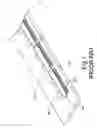
BRIEF DESCRIPTION OF THE DRAWINGSFIG. 1 is a schematic diagram partially showing a perspective view of a packaged structure of a conventional light emitting module;
FIG. 2 is a schematic diagram showing a side view of the packaged structure of FIG. 1;
FIG. 3A is a schematic diagram partially showing a perspective view of a packaged structure of a light emitting module according to a preferred embodiment of the present invention;
FIG. 3B is a partially enlarged view of the portion A in FIG. 3A;
FIG. 4 is a schematic diagram showing a side view of the packaged structure of FIG. 3;
FIG. 5 is a resolving diagram schematically showing a top perspective view of an example of the light emitting module of FIG. 3; and
FIG. 6 is a schematic diagram showing a top perspective view of the assembled structure of FIG. 5.
DETAILED DESCRIPTION OF THE PREFERRED EMBODIMENTReferring to FIG. 3A, a packaged structure of an LED module according to a preferred embodiment is partially shown. The LED module comprises a substrate 311, a plurality of light emitting elements 321 and a plurality of driving circuit chips 331 for driving the light emitting elements 321. The substrate has a trench 312 on a top surface thereof for accommodating the light emitting element. These light emitting elements 321 are mounted into the trench 312 with adhesive material 341 and separate from one another for independently emitting light. The driving circuit chips 331 are then placed above the light emitting elements 321 and the substrate 311, as shown in FIG. 3B. On the bottom surfaces of the driving circuit chips 331, conductive bumps 332 and 333 are arranged for connecting to the light emitting elements 321 and the substrate 311, respectively, as shown in FIG. 4.
FIG. 5 is a resolving diagram schematically showing the bottom surface of the driving circuit chip 331. The driving circuit chip 331 is of a flip chip type. The driving circuit chip 331 is firstly reversed and then put on the light emitting element 321 and substrate 311 in a manner that the conductive bumps 332 and 333 are precisely aligned with the contacts 322 and 313. Accordingly, the conductive bumps 332 on the bottom surface of the driving circuit chip 331 are in direct connection to the contacts 322 on the top surface of the light emitting element 321, and the conductive bumps 333 on the bottom surface of the driving circuit chip 331 are in direct connection to the contacts 313 on the top surface of the substrate 311. The assembled structure is shown in FIG. 6. For enhancing resolution of the LED module, the pitch between two adjacent conductive bumps 333 is reduced. By patterning the contacts 332 and 322 according to a micro-lithographic and etching process, the pitch can be lowered to less than 50 micrometers while maintaining reliable quality.
According to the present invention, the required elements for manufacturing an LED module can be reduced due to the omission of bonding wires. The simplified process of manufacturing the LED module is advantageous of increasing yield, reliability and resolution of the product and reducing the manufacturing cost. Further, taking an A4 size LED printer head for example, it takes about 15 minutes to perform the wire bonding operations 5,000 times according to prior art. In case of a resolution of 1,200 dpi, the number and time of the wire-bonding operations become double. On the contrary, there is no difference in the assembling time of the LED module of the present invention for different resolutions because the contacts can be integrally formed and no bonding operation is required.
For use in an image processing apparatus such as printing machines, copying machines or scanning machines, the substrate mentioned above can be a printed circuit board, and the light emitting element can be a light emitting diode, a liquid crystal display element or a laser light source element. The term “printed circuit board (PCB)” used herein widely indicates a variety of substrates mounted or formed thereon associated circuits. For example, the material of the PCB could be organic material currently used in the art or non-organic such as glass or ceramic.
While the invention has been described in terms of what is presently considered to be the most practical and preferred embodiments, it is to be understood that the invention needs not be limited to the disclosed embodiment. On the contrary, it is intended to cover various modifications and similar arrangements included within the spirit and scope of the appended claims which are to be accorded with the broadest interpretation so as to encompass all such modifications and similar structures.
Claims
What is claimed is:1. A light emitting module, comprising:
a substrate;
a light emitting element attached to said substrate and having a plurality of first contacts on a top surface thereof; and
a driving circuit chip attached onto said substrate and having a plurality of second contacts in direct connection to said first contacts one on one when being placed above said light emitting element.
2. The light emitting module according to claim 1 wherein said substrate has a trench on a top surface thereof for accommodating said light emitting element.
3. The light emitting module according to claim 2 wherein said light emitting element is mounted into said trench with adhesive material.
4. The light emitting module according to claim 2 wherein said top surface of said light emitting element in said trench is substantially at the same level with said top surface of said substrate.
5. The light emitting module according to claim 4 wherein said second contacts and a plurality of third contacts are arranged on a bottom surface of said driving circuit chip, and said third contacts are in direct connection to fourth contacts arranged on said top surface of said substrate when said driving circuit chip is placed above said light emitting element and said substrate.
6. The light emitting module according to claim 5 wherein said second and third contacts are identical conductive bumps formed on both sides of said driving circuit chip, respectively.
7. The light emitting module according to claim 1 wherein said second contacts and a plurality of third contacts are arranged on a bottom surface of said driving circuit chip, and said third contacts are in direct connection to fourth contacts arranged on said top surface of said substrate when said driving circuit chip is placed above said light emitting element and said substrate.
8. The light emitting module according to claim 7 wherein said second and third contacts are conductive bumps.
9. The light emitting module according to claim 1 wherein a pitch between two adjacent ones of said second contacts is less than 50 micrometers.
10. The light emitting module according to claim 1 wherein said substrate is a printed circuit board.
11. The light emitting module according to claim 1 wherein said light emitting element is a light emitting diode, a liquid crystal display element or a laser light source element.
12. The light emitting module according to claim 1 for use in a printing machine, a copying machine or a scanning machine.
13. A light emitting module, comprising:
a substrate having a trench on a first surface thereof;
a light emitting element disposed in said trench and having a plurality of first contacts exposed from said trench; and
a driving circuit chip having a plurality of second contacts electrically connected to said first contacts one on one for driving said light emitting element.
14. The light emitting module according to claim 13 wherein a plurality of third contacts are formed on a bottom surface of said driving circuit chip together with said second contacts and electrically connected to fourth contacts arranged on said first surface of said substrate.
15. The light emitting module according to claim 14 wherein said second and third contacts are conductive bumps arranged on said bottom surface of said driving circuit chip.
16. The light emitting module according to claim 15 wherein said first contacts of said light emitting element in said trench are substantially at the same level with said fourth contacts of said substrate, and said conductive bumps are in direct connection to said first and fourth contacts when said driving circuit chip is placed above said light emitting element and said substrate.
17. The light emitting module according to claim 13 wherein a pitch between two adjacent ones of said second contacts is less than 50 micrometers.
18. The light emitting module according to claim 13 wherein said substrate is a printed circuit board.
19. The light emitting module according to claim 13 wherein said light emitting element is a light emitting diode, a liquid crystal display element or a laser light source element.
20. A light emitting module, comprising:
a substrate having a trench on a top surface thereof, a plurality of contacts being arranged on said top surface of said substrate beside said trench;
a light emitting element having a bottom surface attached to said substrate in said trench and a top surface exposed from said trench, a plurality of contacts being arranged on said top surface of said light emitting element, which are substantially at the same level with said contacts of said substrate; and
a driving circuit chip having a plurality of first conductive bumps in direct connection to said contacts of said light emitting element and a plurality of second conductive bumps in direction connection to said contacts of said substrate when said driving circuit chip is placed above said light emitting element and said substrate.
Images & Drawings included:


Sources:
- United States Patent and Trademark Office - verify current appl. status at the USPTO↗
Similar patent applications:
- » 20180277729
LIGHT-EMITTING MODULE SUBSTRATE, LIGHT-EMITTING MODULE, SUBSTRATE FOR LIGHT-EMITTING MODULE HAVING COOLER, AND PRODUCTION METHOD FOR LIGHT-EMITTING MODULE SUBSTRATE - » 20230115310
METHOD FOR ESTIMATING TEMPERATURE OF LIGHT EMITTING MODULE, LIGHT EMITTING MODULE, AND AUTOMOTIVE UNIT - » 20240399956
METHOD FOR ESTIMATING TEMPERATURE OF LIGHT EMITTING MODULE, LIGHT EMITTING MODULE, AND AUTOMOTIVE UNIT - » 20230071897
Method of manufacturing light emitting module, light emitting module, and projector - » 20200194974
Method of manufacturing light emitting module, light emitting module, and projector - » 20110310590
Light emitting module, light emitting module unit, and backlight system - » 20210005590
Method of manufacturing light emitting device, method of manufacturing light emitting module, light emitting device, and light emitting module - » 20240222940
METHOD OF MANUFACTURING LIGHT EMITTING MODULE, LIGHT EMITTING MODULE, AND PROJECTOR - » 20100073931
LIGHT-EMITTING MODULE, LIGHT-EMITTING DEVICE HAVING THE LIGHT-EMITTING MODULE, AND LIGHTING APPARATUS HAVING THE LIGHT-EMITTING DEVICE - » 20180180252
Light emitting module with concave reflecting structure, display device with light emitting module and method for manufacturing light emitting module with concave reflecting structure
Recent applications in this class:
- » 20250249690 2025-08-07
METHOD FOR ENHANCING OPTICAL PRINTER RESOLUTION - » 20250196511 2025-06-19
EXPOSURE HEAD AND IMAGE FORMING APPARATUS - » 20250065643 2025-02-27
LED CONTROL APPARATUS, IMAGE PRINTING APPARATUS, AND LED CONTROL METHOD - » 20220072871 2022-03-10
LIGHT SOURCE HAVING AT LEAST ONE FIRST LIGHT-EMITTING SEMICONDUCTOR COMPONENT, A FIRST CARRIER ELEMENT AND A DISTRIBUTING ELEMENT - » 20200307251 2020-10-01
Systems and methods of augmenting displays using smart lighting modules - » 20200171842 2020-06-04
POINTER AND INKJET PRINTER INCLUDING POINTER - » 20190329568 2019-10-31
Printing using color changeable material - » 20190168515 2019-06-06
LIGHT-EMITTING ELEMENT ARRAY, AND LIGHT EXPOSURE HEAD AND IMAGE FORMING APPARATUS USING THE SAME - » 20180201028 2018-07-19
Laser printing system - » 20170057247 2017-03-02
Dynamic light emitting diode (LED) print bar positioning system and method