Organic electroluminescent device
US20060115674A1
2006-06-01
11/074,036
2005-03-07
Abstract:
An organic electroluminescent device comprising a light emitting layer including guest material and host material having formula (I):
wherein R1, R2 and R3 individually represent H or substituent, R4 represents alkyl, alkenyl, heteroaryl, aryl group with or without substituent, q is an integer of 0 to 4, m is an integer of 1 to 3, n is an integer of 1 to 3, and m+n=4.
Inventors:
- Tswen-Hsin LIU 13 🇹🇼 Jhudong Township, Taiwan
- Chung-Wen Ko 18 🇹🇼 Sijhih City, Taiwan
- Min-Ling Hung 7 🇹🇼 Kanding Township, Taiwan
Interested in similar patents?
Get notified when new applications in this technology area are published.
Classification:
H05B33/14 » CPC further
Electroluminescent light sources; Light sources with substantially two-dimensional radiating surfaces characterised by the chemical or physical composition or the arrangement of the electroluminescent material, or by the simultaneous addition of the electroluminescent material in or onto the light source
C09K11/06 » CPC main
Luminescent, e.g. electroluminescent, chemiluminescent materials containing organic luminescent materials
H01L51/0094 » CPC further
Solid state devices using organic materials as the active part, or using a combination of organic materials with other materials as the active part; Processes or apparatus specially adapted for the manufacture or treatment of such devices, or of parts thereof; Selection of organic semiconducting materials, e.g. organic light sensitive or organic light emitting materials Silicon-containing organic semiconductors
C09K2211/1007 » CPC further
Chemical nature of organic luminescent or tenebrescent compounds; Non-macromolecular compounds; Carbocyclic compounds Non-condensed systems
C09K2211/1011 » CPC further
Chemical nature of organic luminescent or tenebrescent compounds; Non-macromolecular compounds; Carbocyclic compounds Condensed systems
C09K2211/1014 » CPC further
Chemical nature of organic luminescent or tenebrescent compounds; Non-macromolecular compounds; Carbocyclic compounds bridged by heteroatoms, e.g. N, P, Si or B
C09K2211/1029 » CPC further
Chemical nature of organic luminescent or tenebrescent compounds; Non-macromolecular compounds; Heterocyclic compounds characterised by ligands containing one nitrogen atom as the heteroatom
C09K2211/185 » CPC further
Chemical nature of organic luminescent or tenebrescent compounds; Metal complexes of the platinum group, i.e. Os, Ir, Pt, Ru, Rh or Pd
H01L51/0072 » CPC further
Solid state devices using organic materials as the active part, or using a combination of organic materials with other materials as the active part; Processes or apparatus specially adapted for the manufacture or treatment of such devices, or of parts thereof; Selection of organic semiconducting materials, e.g. organic light sensitive or organic light emitting materials; Macromolecular systems with low molecular weight, e.g. cyanine dyes, coumarine dyes, tetrathiafulvalene aromatic compounds comprising a hetero atom, e.g.: N,P,S; Polycyclic condensed heteroaromatic hydrocarbons comprising only nitrogen in the heteroaromatic polycondensed ringsystem, e.g. phenanthroline, carbazole
H01L51/0085 » CPC further
Solid state devices using organic materials as the active part, or using a combination of organic materials with other materials as the active part; Processes or apparatus specially adapted for the manufacture or treatment of such devices, or of parts thereof; Selection of organic semiconducting materials, e.g. organic light sensitive or organic light emitting materials; Coordination compounds, e.g. porphyrin; Transition metal complexes, e.g. Ru(II)polypyridine complexes comprising Iridium
H01L51/0088 » CPC further
Solid state devices using organic materials as the active part, or using a combination of organic materials with other materials as the active part; Processes or apparatus specially adapted for the manufacture or treatment of such devices, or of parts thereof; Selection of organic semiconducting materials, e.g. organic light sensitive or organic light emitting materials; Coordination compounds, e.g. porphyrin; Transition metal complexes, e.g. Ru(II)polypyridine complexes comprising osmium
H01L51/5012 » CPC further
Solid state devices using organic materials as the active part, or using a combination of organic materials with other materials as the active part; Processes or apparatus specially adapted for the manufacture or treatment of such devices, or of parts thereof specially adapted for light emission, e.g. organic light emitting diodes [OLED] or polymer light emitting devices [PLED] Electroluminescent [EL] layer
Description
BACKGROUNDThe invention relates to an organic electroluminescent device (OLED), and more particularly to a host-guest type OLED.
OLED displays are among the most popular displays. FIG. 1 shows a conventional OLED. Substrate 8 is electrically insulated, comprising transparent glass or plastic materials. Anode 6 is disposed on substrate 8. Organic light emitting layer 4 is interposed between anode 6 and cathode 2. Anode 6 and cathode 2 are connected to external power supply 5. When the anode 6 bias exceeds cathode 2 bias, the diode is in forward bias, thus electrons and holes respectively from anode 6 and cathode 2 are injected into organic light emitting layer 4 to release light.
Phosphorescent efficiency is triple that of the fluorescent efficiency, making phosphorescent material an important OLED element.
A guest material can additionally be added to the light emitting layer to tune light color and luminescent efficiency.
A common host material used in OLEDs is 4,4′-N,N′-dicarbazole-biphenyl (CBP). However, electrons and holes have different transport speeds in CBP. This situation decreases OLED carrier recombination efficiency.
To resolve these and other problems, a better host material is desirable.
SUMMARYAccordingly, the invention provides an organic electroluminescent device.
An organic electroluminescent device comprises a light emitting layer including guest material and host material having formula (I):
-
- wherein R1, R2 and R3 individually represent H or a substituent, R4 represents alkyl, alkenyl, heteroaryl, aryl group with or without a substituent, q is an integer of 0 to 4, m is an integer of 1 to 3, n is an integer of 1 to 3, and m+n=4.
The invention can be more fully understood by reading the subsequent detailed description and examples with references made to the accompanying drawings, wherein:
FIG. 1 is a cross section of a conventional OLED
FIG. 2 is a cross section an OLED of the embodiments;
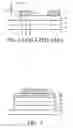
FIG. 3 shows OLED luminescent efficiency of an example and a comparative example; and
FIG. 4 shows OLED lifetime of an example and a comparative example.
DETAILED DESCRIPTIONThe embodiments provide a host material having a silane compound represented by a following formula (I):
In formula (I), R1, R2 and R3 individually represent H or a substituent, comprising C1-C20 alkyl, such as methyl, ethyl, isopropyl, tert-butyl, n-octyl, n-decyl, n-hexadecyl, cyclopropryl, cyclopentyl or cyclohexyl groups; C2-C20 alkenyl; C2-C20 alkynyl, such as propargyl or 3-pentylnyl groups; C1-C20 heteroalkyl; C3-C40 aryl, such as phenyl, o-methylphenyl or naphthyl groups; C3-C40 heteroaryl, such as those containing one or more heteroatoms of oxygen, sulfur or nitrogen, with examples including imidazolyl, pyridyl, furyl, piperidyl, benzoxazolyl, thienyl, triazolyl or carbazolyl groups.
In formula (I), R4 represents C1-C20 alkyl, such as methyl, ethyl, isopropyl, n-octyl, n-decyl, n-hexadecyl, cyclopropryl, cyclopentyl or cyclohexyl groups; C2-C20 alkenyl, such as ethene, propylene, 2-octylene, 3-pentylene groups with or without substituent; C1-C50 heteroaryl, such as host containing one or more heteroatoms of oxygen, sulfur or nitrogen atoms, with examples including imidazolyl, pyridyl, furyl, piperidyl, benzoxazolyl, thienyl or triazolyl groups; C6-C30 aryl, such as phenyl, p-methylphenyl or naphthyl groups.
In formula (I), q is an integer of 0 to 4, m is an integer of 1 to 3, n is an integer of 1 to 3, and m+n=4.
Furthermore, R2 and R3 may combine covalently to form heteroaryl group.
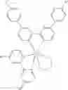
Examples of the host materials include:
Light emitting layer 18 further comprises a guest material represented by the following formula (III) to emit red, green or blue light:
-
- wherein M is a metal having an atomic weight more than 40, r is an integer at least 1, s is an integer at least 0, R5 represents H or C1-C20 alkyl, C2-C20 alkenyl, C2-C20 alkynyl, C1-C20 heteroalkyl, C3-C40 aryl, C3-C40 heteroaryl, X represents auxiliary ligand, A represents aryl or heteroaryl group, B represents aryl group.
Some guest materials used with the sliane compound of the invention for emitting red light include:
-
- wherein R6 represents
Some guest materials used with the sliane compound of the invention for emitting green light include:
Some guest materials used with the sliane compound of the invention for emitting blue light include:
ExampleThe compound (II) synthesis mechanism proceeds as follows:
4.65 g 1,3-Dibromobenzene, 150 ml tetrahydrofurane and 8 ml n-Butyllithium were added to a flask at −78° C . 2 g dichlorodiphenylsilane was added to the flask in N2 and stirred. 200 ml dichloromethane and 200 ml water were added to separate the organic layer. After concentration and purifyication, bis(3-bromo-phenyl)-diphenyl silane (compound 1) was obtained.
0.94 g carbazole, 0.59 g sodium t-butoxide, 0.12 g tri-t-butylphosphine, 0.034 g palladium acetate and 100 ml toluenewere added to a flask. 1.26 g compound 1 was added in the flask to N2, stirred and refluxed. 200 ml dichloromethane and 200 ml water were added to separate the organic layer. After concentration and purifyication, compound 2 was obtained.
Referring to FIG. 2, 60˜80 nm hole injection layer 22, 20˜40 nm hole transport layer 24, 20˜40 nm compound (II) light emitting layer 26, 10˜25 nm hole blocking layer 28, 30˜35 nm electron transport layer 30 and cathode 32 were evaporated on the ITO substrate 20 sequentially to form an organic electroluminescent device. The organic light emitting layer 26 was co-doped with a guest material.
OLED luminescent efficiency reaches 7.3 cd/A, as shown in FIG. 3 line B, with lifetime of 166 hours of 20% decay, as shown in FIG. 4 line B.
Comparative ExampleFabrication of this OLED is the same as the example, except for the CBP light emitting layer.
OLED luminescent efficiency reaches 5.5 cd/A, as shown in FIG. 3 line A, with lifetime is 162 hours of 30% decay, as shown in FIG. 4 line A.
Accordingly, the present invention OLED provides better luminescent efficiency and longer lifetime than conventional OLEDs.
While the invention has been described by way of example and in terms of preferred embodiment, it is to be understood that the invention is not limited thereto. To the contrary, it is intended to cover various modifications and similar arrangements (as would be apparent to those skilled in the art). Therefore, the scope of the appended claims should be accorded the broadest interpretation to encompass all such modifications and similar arrangements.
Claims
What is claimed is:1. An organic electroluminescent device, comprising:
an anode and cathode pair; and
a light emitting layer interposed between the anode and cathode pair, wherein the light emitting layer comprises a host material and a guest material, wherein the host material comprises a silane compound respected by formula (I):
wherein R1, R2 and R3 individually represent H or a substituent; R4 represents alkyl, alkenyl, heteroaryl, or aryl group, each with or without substituent; q is an integer of 0 to 4, m is an integer of 1 to 3, n is an integer of 1 to 3, and m+n=4.
2. The organic electroluminescent device as claimed in claim 1, wherein the R2 and R3 combine covalently to form heteroaryl.
3. The organic electroluminescent device as claimed in claim 1, wherein the silane compound comprises formula (II):
4. The organic electroluminescent device as claimed in claim 1, comprising:
a hole injection layer between the light emitting layer and the anode;
a hole transport layer between the hole injection layer and the light emitting layer;
a hole blocking layer between the light emitting layer and the cathode; and
an electron transport layer between the hole blocking layer and the cathode.
5. The organic electroluminescent device as claimed in claim 1, wherein the guest material comprises formula (III):
wherein M is a metal having an atomic weight exceeding 40; r is an integer at least 1; s is an integer at least 0; R5 represents H or substituent; X represents auxiliary ligand; A represents aryl or heteroaryl group; B represents aryl group.
6. The organic electroluminescent device as claimed in claim 5, wherein the guest material comprises formula:
wherein R6 represents
7. The organic electroluminescent device as claimed in claim 5, wherein the guest material comprises formula:
Images & Drawings included:


Sources:
- United States Patent and Trademark Office - verify current appl. status at the USPTO↗
Similar patent applications:
- » 20050186698
Method of manufacturing organic electroluminescent device, organic electroluminescent device, substrate for organic electroluminescent device, and electronic apparatus - » 20180342681
Light-emitting material for organic electroluminescent device, organic electroluminescent device using same, and material for organic electroluminescent device - » 20160064675
Light-emitting material for organic electroluminescent device, organic electroluminescent device using same, and material for organic electroluminescent device - » 20140008641
Light-emitting material for organic electroluminescent device, organic electroluminescent device using same, and material for organic electroluminescent device - » 20180019404
Light-emitting material for organic electroluminescent device, organic electroluminescent device using same, and material for organic electroluminescent device - » 20070152565
Light-emitting material for organic electroluminescent device, organic electroluminescent device using same, and material for organic electroluminescent device - » 20100181555
Material for organic electroluminescent device, organic electroluminescent device, and organic electroluminescent display - » 20190245154
Organic electroluminescent device, organic electroluminescent display device including the same, and organometallic compound for organic electroluminescent device - » 20120001124
Ink for organic electroluminescent device, manufacturing method of organic electroluminescent device, organic display panel, organic display apparatus, organic electroluminescent apparatus, ink, forming method of functional layer, and organic electroluminescent device - » 20120032152
Asymmetrical aryl amine derivative for organic electroluminescence devices, method for preparing same, organic thin film for organic electroluminescence devices and organic electroluminescence device using same
Recent applications in this class:
- » 20250171685 2025-05-29
ORGANIC ELECTROLUMINESCENT MATERIALS AND DEVICES - » 20250171684 2025-05-29
AROMATIC HETREOCYCLES FOR ORGANIC ELECTROLUMINESCENT DEVICES - » 20250171683 2025-05-29
EMISSION MATERIAL, AND ORGANIC ELECTROLUMINESCENT DEVICE - » 20250163319 2025-05-22
COMPOUND FOR ORGANIC ELECTRIC ELEMENT, ORGANIC ELECTRIC ELEMENT USING THE SAME, AND AN ELECTRONIC DEVICE THEREOF - » 20250163318 2025-05-22
FUNCTIONALIZED CARBON NANOTUBE COMPOSITE BIOMATERIALS AND METHODS THEREOF - » 20250163317 2025-05-22
ORGANIC ELECTROLUMINESCENT MATERIALS AND DEVICES - » 20250163316 2025-05-22
OH GROUP-CONTAINING PHOSPHOR-FLUORESCENT MATERIAL INCLUDING VALLEYTRONICS MATERIAL AND FLUORESCENT ORGANIC MATERIAL - » 20250154407 2025-05-15
ORGANIC ELECTROLUMINESCENT DEVICE, DISPLAY APPARATUS AND COMPOSITION - » 20250154406 2025-05-15
ORGANIC COMPOUND AND OLED HAVING SAME AND ORGANICA LIGHT-EMITTING APPARATUS - » 20250154405 2025-05-15
ORGANOMETALLIC COMPOUND, ORGANIC LIGHT-EMITTING DEVICE INCLUDING THE SAME, AND ELECTRONIC APPARATUS INCLUDING ORGANIC LIGHT-EMITTING DEVICE