Differential clock correction
US20060132207A1
2006-06-22
11/020,984
2004-12-22
✅ Patent granted
US 7,265,597 B2
2007-09-04
-
-
Kenneth B. Wells | Hai L. Nguyen
2025-03-11
Abstract:
A method, system, and apparatus are disclosed that correct a differential clock signal. A clock correction circuit may determine a DC correction for a first clock signal of a differential clock signal and a DC correction for a second clock signal of a differential clock signal based upon a DC level of the differential clock signal. The clock correction circuit may adjust a DC level of the first clock signal based upon the DC correction for the first clock signal and a DC level of the second clock signal based upon the DC correction for the second clock signal to substantially maintain a duty cycle of the differential clock signal.
Assignee:
- INTEL CORPORATION 47,158 🇺🇸 Santa Clara, CA, United States
Interested in similar patents?
Get notified when new applications in this technology area are published.
Classification:
H03K5/1565 » CPC main
Manipulating of pulses not covered by one of the other main groups of this subclass; Arrangements in which a continuous pulse train is transformed into a train having a desired pattern the output pulses having a constant duty cycle
H03K5/003 » CPC further
Manipulating of pulses not covered by one of the other main groups of this subclass Changing the DC level
H03K3/017 IPC
Circuits for generating electric pulses; Monostable, bistable or multistable circuits; Details Adjustment of width or dutycycle of pulses
Description
BACKGROUND OF THE INVENTIONWireless transmission systems may have transceivers to modulate and demodulate signals based upon a differential clock signal. For some modulation techniques, accuracy of modulating and demodulating is dependent upon the accuracy of the differential clock signal. In particular, some modulation techniques require a differential clock signal with a 50 percent duty cycle.
BRIEF DESCRIPTION OF THE DRAWINGSThe invention described herein is illustrated by way of example and not by way of limitation in the accompanying figures. For simplicity and clarity of illustration, elements illustrated in the figures are not necessarily drawn to scale. For example, the dimensions of some elements may be exaggerated relative to other elements for clarity. Further, where considered appropriate, reference labels have been repeated among the figures to indicate corresponding or analogous elements.
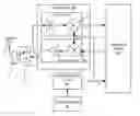
FIG. 1 illustrates an embodiment of a wireless system with a clock correction circuit.
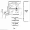
FIG. 2 illustrates an embodiment of the clock correction circuit of FIG. 1.
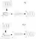
FIG. 3 illustrates correction of a differential clock signal with a duty cycle greater than 50 percent.
FIG. 4 illustrates correction of a differential clock signal with a duty cycle less than 50 percent.
DETAILED DESCRIPTION OF THE INVENTIONIn the following detailed description, numerous specific details are described in order to provide a thorough understanding of the invention. However the present invention may be practiced without these specific details. In other stances, well known methods, procedures, components and circuits have not been described in detail so as not to obscure the present invention. Further, example sizes/models/values/ranges may be given, although the present invention is not limited to these specific examples.
References in the specification to “one embodiment”, “an embodiment”, “an example embodiment”, etc., indicate that the embodiment described may include a particular feature, structure, or characteristic, but every embodiment may not necessarily include the particular feature, structure, or characteristic. Moreover, such phrases are not necessarily referring to the same embodiment. Further, when a particular feature, structure, or characteristic is described in connection with an embodiment, it is submitted that it is within the knowledge of one skilled in the art to affect such feature, structure, or characteristic in connection with other embodiments whether or not explicitly described.
Referring to FIG. 1 an embodiment of a wireless system is shown. The wireless system may include an antenna 4, filter 8, a switch 12, a transceiver 16, a baseband circuit 20, a clock correction circuits 24, and a clock generator 28. The antenna 4 may receive wireless modulated signals from the environment and provide the transceiver 16 with the received modulated signal via the filter 8 and the switch 12. The transceiver 16 may comprise a receiver 32 to demodulate the modulated signal and to obtain a baseband signal. To this end, the receiver 32 may comprise an amplifier 36 to amplify the modulated signal received by the antenna 4. Further, the receiver 32 may comprise a demodulator 40 to demodulate the amplified modulated signal and provide the baseband circuit 20 with a baseband signal for further processing. In one embodiment, the demodulator 40 comprises an Orthogonal Frequency Division Multiplexing (OFDM) demodulator that demodulates the modulated signal based upon a corrected differential clock signal of the clock correction circuit 24.
The transceiver 16 may further comprise a transmitter 44 to modulate a baseband signal of the baseband circuit 20 to obtain a modulated signal that is representative of the baseband signal. To this end, the transmitter 44 may comprise a modulator 48 to modulate a baseband signal of baseband circuit 20. Further, the transmitter 44 may comprise an amplifier 52 to amplify the modulated signal of the modulator 48 and provide the amplified signal to the antenna 4 via the switch 12 and the filter 8. In one embodiment, the modulator 48 comprises an Orthogonal Frequency Division Multiplexing (OFDM) modulator that modulates the baseband signal based upon a corrected differential clock signal of the clock correction circuit 24.
The clock generator 28 may generate a differential clock signal that comprises a positive or first clock signal IP and a negative or second clock signal IN that is a mirror image of the first clock signal IP. Ideally, crossings of the first clock signal IP and the second clock signal IN define periods of equal lengths which is commonly referred to as a 50 percent duty cycle. Accuracy of certain modulation and demodulation techniques (e.g. OFDM (de)modulation) are dependent upon the ability to maintain a differential clock signal at a 50 percent duty cycle. However, variation in temperature, process, nonlinearity of devices, mismatches may result in a shift in the duty cycle of the differential clock signal IN and IP which is more pronounced when the differential clock signal operates at a small amplitudes (e.g. millivolt range). Accordingly, the clock correction circuit 24 may adjust or correct the differential clock signal of the clock generator 28 in order to obtain a corrected clock signal that substantially maintains a 50 percent duty cycle.
Referring now to FIG. 2, an embodiment of the clock correction circuit 24 is shown. The clock correction circuit 24 according to an embodiment may comprise a correction generation circuit 60. The correction generation circuit 60 may generate a correction signal ICP for a positive clock signal IP of the differential clock signal and a correction signal ICN for a negative clock signal IN of the differential clock signal. In one embodiment, the correction generation circuit 60 may comprise a direct current (DC) level detector 62, a bias circuit 64, and a current divider 66. The DC level detector 62 may generate a DC voltage Vcp that is indicative of the DC level of the positive clock signal IP of the differential clock signal. In one embodiment, the DC level detector 62 may comprise a low pass filter (e.g. a resistor and a capacitor) that filters out the AC (alternating current) portion of the positive clock signal IP and allows the DC portion of the positive clock signal IP to pass. As a result, the output of the low pass filter may comprise a DC voltage that is proportional to the DC level of the positive clock signal IP.
The bias circuit 64 may generate a bias current IBIAS that has a DC current level that is based upon the DC voltage Vcp of the DC level detector 62. To this end, the bias circuit 64 in one embodiment comprises an operational amplifier, a resistor RBIAS, a transistor MBIAS that are connected in a classical voltage to current amp. In the depicted configuration, the operational amplifier, the resistor RBIAS, and the transistor MBIAS may generate a bias current IBIAS that is negatively proportional to the DC voltage Vcp of the positive clock signal IP, generated by the DC level detector 62.
The current divider 66 may generate the correction signals ICP, ICN for the clock signals IP, IN based upon the bias current IBIAS of the bias circuit 64. To this end, the current divider 66 in one embodiment may comprise a reference current source CREF and transistors MP, MN. The transistors MP, MN may divide a reference current IREF of the reference current source CREF based upon the bias current IBIAS. In particular, the transistor MN may generate a correction signal ICN for the negative clock signal IN that is a mirror of the bias current IBIAS. In response to the transistor MN generating a correction signal ICN of IBIAS, the transistor MP may generate a correction signal ICP for the positive clock signal IP that has a DC level equal to the reference current IREF minus the bias current ICN. In one embodiment, the reference current source CREF and the bias circuit 64 are configured such that bias circuit 64 generates a bias current IBIAS of I0 and the reference current source CREF generates a reference current IREF of 2*I0 when the clock signals IP, IN of the differential clock signal generate a 50 percent duty cycle.
As depicted, the clock correction circuit 24 may further comprise a level shifter 70 and an output buffer 80. The level shifter 70 may shift the DC level of the clock signals IP, IN based upon the corresponding correction signals ICP, ICN. In one embodiment, the level shifter 70 may comprise controllable current sources CP, CN and transistors MP, MN. The current sources CP, CN may generate DC correction currents IDCP, IDCN that are proportional to the correction signals ICP, ICN. In particular, the current sources CP, CN may respectively generate their DC correction currents IDCP, IDCN such that they are equal to the correction signals ICP, ICN times a gain factor A (e.g. 1). Furthermore, the current sources CP, CN in one embodiment are matched such that the current sources CP, CN generate substantially identical DC currents IDCP, IDCN for substantially identical correction signals ICP, ICN. The transistors MP, MN may respectively receive the clock signals IP, IN via their gates and the correction signal ICP, ICN via their sources thereby producing level shifted output currents IOP, ION.
The output buffer 80 may generate a corrected clock signal OP, ON based upon the shifted output currents IOP, ION of the level shifter 70. As shown, the output buffer 80 may comprise transistors MOP, MON, resistors ROP, RON, and a current source CO that form a current-mode logic buffer. The resistor ROP, transistor MOP, and current source CO may generate, based upon the shifted output current IOP, a corrected positive clock signal OP with a DC offset of substantially zero volts. Similarly, the resister RON, transistor MON, and current source CO may generate, based upon the shifted output current ION, a corrected negative clock signal On with a DC offset of substantially zero volts.
Operation of the clock correction circuit 24 when the differential clock signal has a duty cycle of more than 50 percent will now be described in regard to FIG. 3. When the differential clock signal has a duty cycle of more than 50 percent, the positive clock signal IP may have a positive DC offset. In one embodiment, the DC level detector 62 may generate a reference DC voltage Vcp0 when the differential clock signal has a 50 percent duty cycle. Therefore, the DC level detector 62 in response to the positive clock signal may generate a larger DC voltage Vcp (e.g. Vcp0+ΔVcp) than the reference DC voltage Vcp0 since the positive clock signal has a positive DC offset. In particular, the larger DC voltage Vcp may comprise the reference DC voltage Vcp0 and a DC offset ΔVcp.
The bias circuit 64 in turn may generate a smaller bias current IBIAS (e.g. I0−ΔI) than when the differential clock signal has a 50 percent duty cycle. In particular, the bias current IBIAS may comprise the reference bias current 10 and a bias offset ΔI that is negative and proportional to the DC offset ΔVcp. The transistor MN may generate a smaller correction signal IcN (e.g. I0−ΔI) by mirroring the smaller bias current IBIAS. As a result of generating a smaller correction signal IcN for the negative clock signal IN, the transistor MP may generate a larger correction signal ICP (e.g. I0+ΔI) for the positive clock signal IP.
The controllable current sources CP may increase the DC correction current IDCP for the positive clock signal IP based upon the larger correction signals ICP. Conversely, the controllable current sources CN may reduce the DC correction current IDCN for the negative clock signal based upon the smaller correction signals ICN. In particular, the current sources CP, CN may respectively generate a larger DC correction current IDCP (e.g. I0+ΔI) and a smaller DC correction current (e.g. I0−ΔI). The larger DC correction current IDCP effectively causes the level shifter 70 to shift the DC level of the output lop downward, and the smaller DC correction current IDCN effectively causes the level shifter 70 to shift the DC level of the output ION upward to obtain a differential clock signal having a 50 percent duty cycle at the outputs OP and ON of the output buffer 80.
Operation of the clock correction circuit 24 when the differential clock signal has a duty cycle of less than 50 percent will now be described in regard to FIG. 4. When the differential clock signal has a duty cycle of less than 50 percent, the positive clock signal IP may have a negative DC offset. Therefore, the DC level detector 62 in response to the positive clock signal may generate a smaller DC voltage Vcp (e.g. Vcp0−ΔVcp) than the reference DC voltage Vcp0 since the positive clock signal has a negative DC offset. In particular, the smaller DC voltage Vcp may comprise the reference DC voltage Vcp0 and a negative DC offset ΔVcp.
The bias circuit 64 in turn may generate a larger bias current IBIAS (e.g. I0+ΔI) than when the differential clock signal has a 50 percent duty cycle. In particular, the bias current IBIAS may comprise the reference bias current I0 and a bias offset ΔI that is negatively proportional to the DC offset ΔVcp. The transistor MN may generate a larger correction signal ICN (e.g. I0+ΔI) by mirroring the larger bias current IBIAS As a result of generating a larger correction signal ICN for the negative clock signal IN, the transistor MP may generate a smaller correction signal IP (e.g. I0−ΔI) for the positive clock signal IP.
The controllable current sources CP may decrease the DC correction current IDCP for the positive clock signal IP based upon the smaller correction signals ICP. Conversely, the controllable current sources CN may increase the DC correction current IDCN for the negative clock signal based upon the larger correction signals ICN. In particular, the current sources CP, CN may respectively generate a smaller DC correction current IDCP (e.g. I0−ΔI) and a larger DC correction current IDCN (e.g. I0+ΔI). The smaller DC correction current IDCP effectively causes the level shifter 70 to shift the DC level of the output lop upward, and the larger DC correction current IDCN effectively causes the level shifter 70 to shift the DC level of the output ION downward to obtain a differential clock signal having a 50 percent duty cycle at the outputs OP and ON of the output buffer 80.
Certain features of the invention have been described with reference to example embodiments. However, the description is not intended to be construed in a limiting sense. Various modifications of the example embodiments, as well as other embodiments of the invention, which are apparent to persons skilled in the art to which the invention pertains are deemed to lie within the spirit and scope of the invention.
Claims
What is claimed is:1. A method comprising
determining a DC correction for a first clock signal of a differential clock signal and a DC correction for a second clock signal of a differential clock signal based upon a DC level of the differential clock signal, and
adjusting a DC level of the first clock signal based upon the DC correction for the first clock signal and a DC level of the second clock signal based upon the DC correction for the second clock signal to substantially maintain a duty cycle of the differential clock signal.
2. The method of claim 1 wherein adjusting substantially maintains the duty cycle of the differential clock signal at substantially a 50 per cent duty cycle.
3. The method of claim 1 wherein adjusting comprises
increasing a DC voltage level of the first clock signal based upon the DC correction for the first clock signal, and
decreasing a DC voltage level of the second clock signal based upon the DC correction for the second clock signal.
4. The method of claim 1 wherein determining comprises dividing a reference current based upon the DC level of the first clock signal to obtain a first correction signal indicative of the DC correction for the first clock signal and to obtain a second correction signal indicative of the DC correction for the second clock signal.
5. The method of claim 4 wherein adjusting comprises
shifting the DC level of the first clock signal based upon the first correction signal, and
shifting the DC level of the second clock signal based upon the first correction signal.
6. The method of claim 1 further comprising generating a corrected differential signal comprising a predetermined duty cycle and a predetermined AC magnitude.
7. An apparatus comprising:
a correction generation circuit to generate a first correction signal for a first clock signal of a differential clock signal and to generate a second correction signal for a second clock signal of the differential clock signal, and
a level shifter to adjust a duty cycle of the differential clock signal by shifting a DC level of the first clock signal based the first correction signal, and shifting a DC level of the second clock signal based upon the second correction signal.
8. The apparatus of claim 7 further comprising an output buffer to receive the first clock signal and the second clock signal shifted by the level shifter and to output a corrected differential clock signal having substantially the predetermined duty cycle and substantially a predetermined AC magnitude.
9. The apparatus of claim 7 wherein the correction generation circuit generates the first correction signal and the second correction signal based upon a DC level of the first clock signal.
10. The apparatus of claim 7 wherein
the correction generation circuit comprises a low pass filter to receive the first clock signal and to generate a DC voltage indicative of a DC level of the first clock signal, and
the correction generation circuit generates the first correction signal and the second correction signal based upon the DC voltage of the low pass filter.
11. The apparatus of claim 7 wherein the correction generation circuit divides a reference current into the first correction signal and the second correction signal based upon a DC level of the first clock signal.
12. The apparatus of claim 7 wherein the correction generation circuit comprises
a DC level detector to receive the first clock signal and to generate a DC voltage indicative of the DC level of the first clock signal,
a bias circuit to generate a bias current that is based upon the DC voltage of the low pass filter, and
a current divider to divide a reference current into the first correction signal and the second correction signal based upon the bias current.
13. The apparatus of claim 7 wherein the level shifter shifts a DC level of the first clock signal and the DC level of the second clock signal to maintain the duty cycle of the differential clock signal at a substantially 50 per cent duty cycle.
14. A system comprising
a differential clock to generate a differential clock signal comprising a first clock signal and a second clock signal, and
a clock correction circuit to generate a corrected differential clock signal with the first clock signal and the second clock signal DC level shifted such that the corrected differential clock signal substantially has a predetermined duty cycle.
15. The system of claim 14 further comprising a transmitter to wirelessly transmit signals based upon the corrected differential clock signal.
16. The system of claim 14 further comprising a receiver to wirelessly receive signals based upon the corrected differential clock signal.
17. The system of claim 14 further comprising an orthogonal frequency division multiplexing transceiver to wirelessly transmit and receive signals based upon the corrected differential clock signal.
18. The system of claim 14 further comprising
at least one antenna, and
an orthogonal frequency division multiplexing transceiver to transmit and receive signals based upon the corrected differential clock signal via the at least one antenna.
19. The system of claim 14 further comprising a transceiver that operates based upon the corrected differential clock signal, wherein
the clock correction circuit shifts a DC voltage level of the first clock signal and a DC voltage level of the second clock signal to substantially maintain the predetermined duty cycle.
20. The system of claim 14 further comprising a transceiver that operates based upon the corrected differential clock signal, wherein the clock correction circuit shifts a DC level of the first clock signal and a DC level of the second clock signal based upon a determined DC voltage level of the first clock signal to maintain the predetermined duty cycle at substantially at a 50 per cent duty cycle.
Images & Drawings included:
Sources:
- United States Patent and Trademark Office - verify current appl. status at the USPTO↗
Similar patent applications:
- » 16791071
Differential clock duty cycle correction with hybrid current injectors and tapered digital to analog converter - » 16916309
Differential clock duty cycle correction with hybrid current injectors and tapered digital to analog converter - » 20070159224
Duty-cycle correction circuit for differential clocking - » 20070285139
Amplifier Circuit and Method for Correcting the Duty Ratio of a Differential Clock Signal - » 20210167766
Duty cycle and skew measurement and correction for differential and single-ended clock signals - » 20050024263
Method for generating clock corrections for a wide-area or global differential GPS system
Recent applications in this class:
- » 20250279774 2025-09-04
DUTY CYCLE CORRECTION CIRCUIT - » 20250274112 2025-08-28
CLOCK SIGNAL DUTY RATIO CORRECTION CIRCUIT AND METHOD OF CORRECTING DUTY RATIO - » 20250211218 2025-06-26
PROGRAMMABLE SELF-BIASING INVERTER FOR CORRECTING DUTY CYCLE DISTORTION - » 20250167778 2025-05-22
SEMICONDUCTOR SYSTEM FOR MONITORING RESULTS OF DETERMINATION OF DUTY RATIO OF DATA CLOCK SIGNALS - » 20250150069 2025-05-08
LOW-NOISE SPEEDY DUTY CYCLE DETECTOR AND METHOD THEREOF - » 20250105832 2025-03-27
DUTY CYCLE CORRECTION METHOD AND DUTY CYCLE CORRECTION SYSTEM - » 20250096785 2025-03-20
APPARATUSES AND METHODS FOR DUTY CYCLE ADJUSTMENT - » 20250070768 2025-02-27
Controlling Duty Cycle Distortion - » 20250047272 2025-02-06
CLOCK DOUBLER AND A SEMICONDUCTOR APPARATUS USING THE SAME - » 20250023557 2025-01-16
DUTY CYCLE CORRECTOR, SEMICONDUCTOR DEVICE INCLUDING THE SAME, AND OPERATING METHOD OF DUTY CYCLE CORRECTOR
Recent applications for this Assignee:
- » 20250294866 2025-09-18
GATE CUT CONFINED WITHIN GATE TRENCH - » 20250294846 2025-09-18
BACKSIDE CROSS-COUPLE INTERCONNECTS - » 20250294835 2025-09-18
ELONGATED VERTICAL STRUCTURES OF CHANNEL MATERIALS - » 20250294827 2025-09-18
CO-INTEGRATION OF GATE-ALL-AROUND DEVICES WITH DIFFERENT NUMBERS OF NANORIBBONS - » 20250294818 2025-09-18
TRANSISTOR DESIGNS FOR FLOATING BODY MEMORY - » 20250294781 2025-09-18
MAGNETIC CORE INDUCTORS ON PACKAGE SUBSTRATES - » 20250294777 2025-09-18
INTEGRATED CIRCUIT DEVICE WITH MEMORY ARRAY AND SHARED GAIN ELEMENT - » 20250293985 2025-09-18
RECEIVER-BASED PRECISION CONGESTION CONTROL - » 20250293860 2025-09-18
PRESERVATION OF CONFIDENTIALITY AND INTEGRITY OF MODELS DURING EXECUTION - » 20250293706 2025-09-18
LOW-RANK DECOMPOSITION-BASED HARDWARE COMPRESSION OF MATRICES AND TENSORS