Solder for device package
US20060138652A1
2006-06-29
11/200,120
2005-08-10
Abstract:
A solder for device packaging including a plurality of cores, and a coating solder mixed with the cores. The cores are formed of a material having a higher thermal conductivity than the coating solder.
Assignee:
- SAMSUNG ELECTRO-MECHANICS CO., LTD. 292 🇰🇷 Gyeonggi-do, South Korea
Interested in similar patents?
Get notified when new applications in this technology area are published.
Classification:
B23K35/0283 » CPC main
Rods, electrodes, materials, or media, for use in soldering, welding, or cutting characterised by mechanical features, e.g. shape for use in welding; Rods, electrodes, wires multi-cored; multiple
B23K35/0222 » CPC further
Rods, electrodes, materials, or media, for use in soldering, welding, or cutting characterised by mechanical features, e.g. shape for use in soldering, brazing
B23K35/262 » CPC further
Rods, electrodes, materials, or media, for use in soldering, welding, or cutting characterised by the composition or nature of the material; Selection of soldering or welding materials proper with the principal constituent melting at less than 400 degrees C Sn as the principal constituent
B23K35/3006 » CPC further
Rods, electrodes, materials, or media, for use in soldering, welding, or cutting characterised by the composition or nature of the material; Selection of soldering or welding materials proper with the principal constituent melting at less than 1550 degrees C Ag as the principal constituent
B23K35/3013 » CPC further
Rods, electrodes, materials, or media, for use in soldering, welding, or cutting characterised by the composition or nature of the material; Selection of soldering or welding materials proper with the principal constituent melting at less than 1550 degrees C Au as the principal constituent
B23K2101/36 » CPC further
Articles made by soldering, welding or cutting Electric or electronic devices
B23K2103/08 » CPC further
Materials to be soldered, welded or cut Non-ferrous metals or alloys
B23K2103/10 » CPC further
Materials to be soldered, welded or cut; Non-ferrous metals or alloys Aluminium or alloys thereof
B23K2103/12 » CPC further
Materials to be soldered, welded or cut; Non-ferrous metals or alloys Copper or alloys thereof
B23K2103/18 » CPC further
Materials to be soldered, welded or cut Dissimilar materials
B23K2103/26 » CPC further
Materials to be soldered, welded or cut; Dissimilar materials Alloys of Nickel and Cobalt and Chromium
B23K2103/50 » CPC further
Materials to be soldered, welded or cut Inorganic material, e.g. metals, not provided for in –
B23K2103/52 » CPC further
Materials to be soldered, welded or cut; Inorganic material, e.g. metals, not provided for in – Ceramics
H01L33/62 » CPC further
Semiconductor devices with at least one potential-jump barrier or surface barrier specially adapted for light emission; Processes or apparatus specially adapted for the manufacture or treatment thereof or of parts thereof; Details thereof characterised by the semiconductor body packages Arrangements for conducting electric current to or from the semiconductor body, e.g. lead-frames, wire-bonds or solder balls
H01L33/641 » CPC further
Semiconductor devices with at least one potential-jump barrier or surface barrier specially adapted for light emission; Processes or apparatus specially adapted for the manufacture or treatment thereof or of parts thereof; Details thereof characterised by the semiconductor body packages; Heat extraction or cooling elements characterized by the materials
H01L33/647 » CPC further
Semiconductor devices with at least one potential-jump barrier or surface barrier specially adapted for light emission; Processes or apparatus specially adapted for the manufacture or treatment thereof or of parts thereof; Details thereof characterised by the semiconductor body packages; Heat extraction or cooling elements the elements conducting electric current to or from the semiconductor body
H01S5/0237 » CPC further
Semiconductor lasers; Structural details or components not essential to laser action; Mountings; Housings; Method for mounting laser chips; Fixing laser chips on mounts by soldering
H01S5/02476 » CPC further
Semiconductor lasers; Structural details or components not essential to laser action; Arrangements for thermal management Heat spreaders, i.e. improving heat flow between laser chip and heat dissipating elements
H01L2924/0002 » CPC further
Indexing scheme for arrangements or methods for connecting or disconnecting semiconductor or solid-state bodies as covered by; Technical content checked by a classifier Not covered by any one of groups , and
H01L2924/00 » CPC further
Indexing scheme for arrangements or methods for connecting or disconnecting semiconductor or solid-state bodies as covered by
H01L23/34 IPC
Details of semiconductor or other solid state devices Arrangements for cooling, heating, ventilating or temperature compensation ; Temperature sensing arrangements
Description
CROSS-REFERENCE TO RELATED PATENT APPLICATIONSThis application claims the benefit of Korean Patent Application No. 10-2004-0112920, filed on Dec. 27, 2004, in the Korean Intellectual Property Office, the disclosure of which is incorporated herein in its entirety by reference.
BACKGROUND OF THE DISCLOSURE1. Field of the Disclosure
The present invention relates to a solder for device packaging, and more particularly, to a solder for high-temperature, high-power device packaging that can improve heat emission.
2. Description of the Related Art
To package a device, such as, a light emitting device (LED), a laser diode (LD), or the like, a solder is generally designed so that the device can be bonded to a submount at a temperature as low as possible. Accordingly, a conventional solder for device packaging has been generally formed of a eutectic alloy that can lower a melting temperature. Examples of the eutectic alloy include an alloy of gold (Au) and tin (Sn), an alloy of tin (Sn) and silver (Ag), etc. These alloys have low eutectic temperatures.
However, such a eutectic alloy has a bad influence upon emission of heat generated by the device because the eutectic alloy has low thermal conductivity. Hence, a new solder that can satisfy melting characteristic and thermal conductivity is required by a high-temperature, high-power device package that is being developed of late.
SUMMARY OF THE DISCLOSUREEmbodiments of the present invention provide a solder for device packaging that can effectively emit heat generated from a device by having a high thermal conductivity.
In embodiments of the present invention, there may be provided a solder for device packaging, including: a plurality of cores; and a coating solder mixed with the cores. The cores may be formed of a material having a higher thermal conductivity than the coating solder.
The coating solder may be formed with a predetermined thickness on surfaces of the cores so that the cores may be coated with the coating solder.
The cores may be formed of a material having a thermal conductivity of 50 W/mK to 1000 W/mK. The cores may be formed of at least one material of palladium (Pd), chrome (Cr), aluminum nitride (AlN), aluminum (Al), copper (Cu), boron nitride (BN) and diamond.
The coating solder may be formed of at least one material selected from an alloy of gold (Au) and tin (Sn), an alloy of Sn and silver (Ag), an ally of lead (Pb) and Sn and Ag.
BRIEF DESCRIPTION OF THE DRAWINGSThe above and other features and advantages of embodiments of the present invention will become more apparent by describing in detail exemplary embodiments thereof with reference to the attached drawings in which:
FIG. 1 is a perspective view of a solder for device packaging according to an embodiment of the present disclosure;
FIG. 2 is a cross-section of the solder of FIG. 1;
FIG. 3 is a cross-section of a unit structure of the solder of FIG. 1;
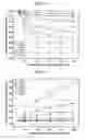
FIGS. 4A through 4F are simulation results showing profiles of internal temperatures of the solder for device packaging of FIG. 1 when a core has thermal conductivity of 50 W/mk, 100 W/mk, 200 W/mk, 315 W/mk, 400 W/mk and 500 W/mk, respectively;
FIG. 5 is a graph showing temperatures of a core, a coating solder, and a heat source versus the thermal conductivity of a core based on the profiles shown in FIGS. 4A through 4F;
FIG. 6 is a graph showing temperatures of a heat source depending on a size of a core; and
FIG. 7 is a graph showing thermal conductivities of the solder for device packaging of FIG. 1 depending on the size of the core.
DETAILED DESCRIPTION OF EXEMPLARY EMBODIMENTS OF THE DISCLOSUREIn embodiments of the present disclosure, a solder for device packaging used to bond a device, such as, a light emitting device (LED), a laser diode (LD), or the like, to a submount may effectively emit heat generated from the device to the submount. The effective heat emission may be achieved by improving the thermal conductivity of the solder. To improve the thermal conductivity of the solder, the solder for device packaging may be formed of a hybrid of an existing solder material and a material having a high thermal conductivity.
More specifically, the solder for device packaging may be comprised of a plurality of cores made of a material having a high thermal conductivity and a coating solder combined with the cores. The cores may be coated with the coating solder having a predetermined thickness. The coating solder may be formed of a material having thermal conductivity lower than that of the cores. A solder for device packaging having a desired melting point, a desired bonding characteristic, and a desired thermal conductivity may be designed by selecting appropriate materials of the cores and the coating solder and adjusting the content of the cores and the content of the coating solder. The solder for device packaging according to the present invention may be used under the same conditions as those under which an existing solder is used.
When a solder for device packaging has a structure as described above, that is, is comprised of cores made of a material having a high thermal conductivity and a coating solder with which the cores are coated, most of the heat generated from a device to be packaged may be exhausted via the cores, thereby improving heat emission compared with a conventional solder. The coating solder improves the bonding characteristic and the melting characteristic, similar to the existing solder.
The coating solder may be formed of the material of an-existing solder. Accordingly, the coating solder may be formed of at least one material selected from the group consisting of an alloy of gold (Au) and tin (Sn), an alloy of Sn and silver (Ag), an ally of lead (Pb) and Sn, and Ag.
The cores may be formed of a material having higher thermal conductivity than a material of the coating solder. The material of the cores may have a thermal conductivity of about 50 to about 1000 W/mK.
Table 1 shows thermal conductivities of various materials.
| TABLE | ||||
| Thermal | Thermal | |||
| conductivity | conductivity | |||
| Material | (W/mK) | Material | (W/mK) | |
| Air | 0.026 | AlN | 170˜230 | |
| Teflon | 0.25 | Al | 237.5 | |
| Glass | 1.4 | Au | 315 | |
| Graphite | 24 | Cu | 400 | |
| GaAs | 46 | BN | 500 | |
| Pd | 73 | Diamond | 500˜600 | |
| (powder) | ||||
| Cr | 94 | Diamond | 1000 | |
Referring to Table 1, the cores may be formed of a material of palladium (Pd), chrome (Cr), aluminium nitride (AlN), aluminium (Al), copper (Cu), boron nitride (BN) and diamond that have thermal conductivity of 50 W/mK or greater. The cores may be formed of a combination of these materials.
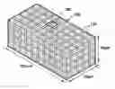
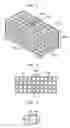
FIG. 1 is a perspective view of a solder for device packaging according to an embodiment of the present invention to which a heat source 100 is attached. FIG. 2 is a cross-section of the solder of FIG. 1. FIG. 3 is a cross-section of a unit structure of the solder of FIG. 1.
Referring to FIGS. 1 through 3, the solder for device packaging according to an embodiment of the present invention may be comprised of a plurality of cores 120 and a coating solder 130. The cores 120 have high thermal conductivity. The coating solder 130 with which each of the cores 120 may be coated. Although the cores 120 may be cubes for convenience of a simulation in the present embodiment, the cores 120 may have various shapes without limiting the present invention. In FIG. 3, reference character C denotes a size of a core when the coating solder 130 is 10 μm in size.
The heat source 100 may be attached to an upper surface of the solder for device packaging. The heat source 100 may be a device that needs to emit heat, such as, an LED, an LD, or the like.
A distribution of an internal temperature of the solder to which the heat source 100 has been attached was measured by a simulation. In the simulation, 0.5 W energy was applied to the heat source 100, and the temperature of a lower surface of the solder was kept constant as 25° C. The coating solder 130 was formed of a material having a thermal conductivity of 50 W/mK.
FIGS. 4A through 4F are simulation results showing profiles of internal temperatures of the solder for device packaging of FIG. 1 when a core has a thermal conductivity of 50 W/mk, 100 W/mk, 200 W/mk, 315 W/mk, 400 W/mk, and 500 W/mk, respectively. The simulation of FIGS. 4A through 4F was conducted when the coating solder 130 was 10 μm in size and the size C of each core is 8 μm. FIG. 5 is a graph showing temperatures of a core, a coating solder, and a heat source versus the thermal conductivity of a core based on the profiles shown in FIGS. 4A through 4F. In FIG. 5, core A denotes a portion of the core 120 that is indicated by A in FIG. 2. Referring to FIGS. 4A through 4F and 5, as the thermal conductivity of the core increases, the temperature of the heat source sharply decreases. Hence, as the thermal conductivity of the core increases, the solder for device packaging according to the present invention can effectively emit heat generated from the device to be packaged.
FIG. 6 is a graph showing temperatures of a heat source depending on a size of a core. FIG. 6 shows the temperatures of the heat source calculated with respect to the thermal conductivity of the core when a size of the coating solder was 10 μm with a variation of the size of the core to 3 μm, 4 μm, 5 μm, 7 μm, 8 μm and 9 μm. Referring to FIG. 6, as the size of the core increases, the temperature of the heat source sharply decreases. For example, when the thermal conductivity of the core was 400 W/mK, and the size of the core was 3 μm, the temperature of the heat source was 476.45° C. However, when the thermal conductivity of the core was still 400 W/mK, and the size of the core was changed to 8 μm, the temperature of the heat source was 253.56° C. Accordingly, as the content of the cores with respect to the coating is high, the solder for device packaging according to the present invention may effectively emit heat generated from a device to be packaged.
FIG. 7 is a graph showing thermal conductivities of the solder for device packaging of FIG. 1 depending on the size of the core. The thermal conductivities of the solder of FIG. 1 were calculated with respect to the thermal conductivity of the core 120 when a size of the coating solder was 10 μm with a variation of the size of the core to 3 μm, 4 μm, 5 μm, 7 μm, 8 μm and 9 μm. Referring to FIG. 7, as the size of the core 120 increases and the thermal conductivity of the core 120 increases, the thermal conductivity of the solder for device packaging increases. For example, when the core 120 was formed of Cu to a size of 9 μm, the thermal conductivity of the solder of FIG. 1 was 161 W/mK. When an existing solder formed of a Pb-Sn alloy having a thermal conductivity of 50 W/mK was used, the temperature of a heat source was 151.71° C. However, when the solder of FIG. 1 having a thermal conductivity of 161 W/mK was used, the temperature of the heat source was 138.56° C. Accordingly, the solder for device packaging of FIG. 1 can reduce the temperature of the heat source by about 9% compared with the existing solder.
As described above, a solder for device packaging according to the present disclosure can effectively emit heat generated from a device by including a plurality of cores formed of a material having a high thermal conductivity and a coating solder with which the cores are coated.
While the present invention has been particularly shown and described with reference to exemplary embodiments thereof, it will be understood by those of ordinary skill in the art that various changes in form and details may be made therein without departing from the spirit and scope of the present invention as defined by the following claims.
Claims
What is claimed is:1. A solder for device packaging, comprising:
a plurality of cores; and
a coating solder mixed with the cores,
wherein the cores are formed of a material having a higher thermal conductivity than the coating solder.
2. The solder for device packaging of claim 1, wherein the coating solder has a predetermined thickness on surfaces of the cores so that the cores are coated with the coating solder.
3. The solder for device packaging of claim 1, wherein the cores are formed of a material having a thermal conductivity of 50 W/mK to 1000 W/mK.
4. The solder for device packaging of claim 3, wherein the cores are formed of at least one material selected from the group consisting of palladium (Pd), chrome (Cr), aluminum nitride (AlN), aluminum (Al), copper (Cu), boron nitride (BN), and diamond.
5. The solder for device packaging of claim 1, wherein the coating solder is formed of at least one material selected from the group consisting of an alloy of gold (Au) and tin (Sn), an alloy of Sn and silver (Ag), an ally of lead (Pb) and Sn, and Ag.
6. The solder for device packaging of claim 1, wherein the solder is used to bond a device that needs to emit heat to a submount.
Images & Drawings included:


Sources:
- United States Patent and Trademark Office - verify current appl. status at the USPTO↗
Similar patent applications:
- » 20140126166
METHOD OF FORMING SOLDER RESIST POST, METHOD OF MANUFACTURING ELECTRONIC DEVICE PACKAGE USONG SOLDER RESIST POST, AND ELECTRONIC DEVICE PACKAGE MANUFACTURED BY USING METHODS - » 20160315072
Package on package (POP) device comprising solder connections between integrated circuit device packages - » 20090127679
POP (package-on-package) device encapsulating soldered joints between external leads - » 20130307157
Semiconductor device packages with solder joint enhancement elements - » 20130009313
Semiconductor device packages with solder joint enhancement element and related methods - » 20230395553
PACKAGE DEVICE PREVENTING SOLDER OVERFLOW - » 20150084150
Ball grid array packaged camera device soldered to a substrate - » 20150262903
Packaged semiconductor devices having solderable lead surfaces exposed by grooves in package compound - » 20160071788
PACKAGED SEMICONDUCTOR DEVICES HAVING SOLDERABLE LEAD SURFACES EXPOSED BY GROOVES IN PACKAGE COMPOUND - » 20160351522
PACKAGE-ON-PACKAGE DEVICE AND CAVITY FORMATION BY SOLDER REMOVAL FOR PACKAGE INTERCONNECTION
Recent applications in this class:
- » 20210276135 2021-09-09
Cable-type welding wire - » 20180056450 2018-03-01
STAINLESS STEEL AUGER BRAID WELDING MATERIAL AND ITS MANUFACTURING METHOD - » 20150209913 2015-07-30
Method and system for additive manufacturing using high energy source and hot-wire
Recent applications for this Assignee:
- » 20230256693 2023-08-17
PLASTIC LENS, METHOD FOR MANUFACTURING PLASTIC LENS, AND MOLDING APPARATUS FOR MANUFACTURING PLASTIC LENS - » 20220322527 2022-10-06
Connection structure embedded substrate and substrate structure including the same - » 20210159015 2021-05-27
Composite electronic component - » 20190295763 2019-09-26
Inductor and method of manufacturing the same - » 20180033746 2018-02-01
Electronic component package - » 20170178984 2017-06-22
Electronic component package and method of manufacturing the same - » 20160035965 2016-02-04
PZT-BASED PIEZOELECTRIC CERAMIC MATERIAL AND PIEZOELECTRIC DEVICE USING THE SAME - » 20160007449 2016-01-07
Chip embedded substrate - » 20160006555 2016-01-07
INTEGRATED FRONT MODULE OF SET TOP BOX - » 20150355219 2015-12-10
MULTI-AXIS SENSOR