Printed wires arrangement for in-line memory (IMM) module
US20060170097A1
2006-08-03
11/227,161
2005-09-16
✅ Patent granted
US 7,394,160 B2
2008-07-01
-
-
Jerome Jackson | Jami M Valentine
2025-09-16
Abstract:
An inline memory module (IMM) architecture may include: a printed circuit board (PCB); a first array of memory devices on a first side of the PCB; a second array of memory devices on a second side of the PCB; at least some of the memory devices of the first array being arranged so as to substantially overlap, relative to a reference axis of the PCB, positional-twin memory devices of the second array, respectively; and multiple vias at least some of which are parts of respective signal paths that connect signal leads of a first memory device in the first array to corresponding signal leads of a second memory device in the second array that is adjacent to a positional-twin third memory device in the second array corresponding to the first memory device.
Assignee:
- SAMSUNG ELECTRONICS CO., LTD. 16,784 🇰🇷 Gyeonggi-Do, South Korea
Interested in similar patents?
Get notified when new applications in this technology area are published.
Classification:
H05K1/181 » CPC main
Printed circuits; Printed circuits structurally associated with non-printed electric components associated with surface mounted components
H05K1/181 » CPC main
Printed circuits; Printed circuits structurally associated with non-printed electric components associated with surface mounted components
G11C5/00 » CPC further
Details of stores covered by group
H01L2224/16 » CPC further
Indexing scheme for arrangements for connecting or disconnecting semiconductor or solid-state bodies and methods related thereto as covered by; Means for bonding being attached to, or being formed on, the surface to be connected, e.g. chip-to-package, die-attach, "first-level" interconnects; Manufacturing methods related thereto; Bump connectors; Manufacturing methods related thereto; Structure, shape, material or disposition of the bump connectors after the connecting process of an individual bump connector
H01L2924/01019 » CPC further
Indexing scheme for arrangements or methods for connecting or disconnecting semiconductor or solid-state bodies as covered by; Chemical elements Potassium [K]
H01L2924/01057 » CPC further
Indexing scheme for arrangements or methods for connecting or disconnecting semiconductor or solid-state bodies as covered by; Chemical elements Lanthanum [La]
H05K2201/10545 » CPC further
Indexing scheme relating to printed circuits covered by; Details of components or other objects attached to or integrated in a printed circuit board; Details of mounted components; Involving several components Related components mounted on both sides of the PCB
H05K2201/10545 » CPC further
Indexing scheme relating to printed circuits covered by; Details of components or other objects attached to or integrated in a printed circuit board; Details of mounted components; Involving several components Related components mounted on both sides of the PCB
H05K2201/10689 » CPC further
Indexing scheme relating to printed circuits covered by; Details of components or other objects attached to or integrated in a printed circuit board; Details of electrical connections of non-printed components, e.g. special leads; Components characterised by their electrical contacts Leaded Integrated Circuit [IC] package, e.g. dual-in-line [DIL]
Y02P70/50 » CPC further
Climate change mitigation technologies in the production process for final industrial or consumer products Manufacturing or production processes characterised by the final manufactured product
Y02P70/50 » CPC further
Climate change mitigation technologies in the production process for final industrial or consumer products Manufacturing or production processes characterised by the final manufactured product
H01L2924/00014 » CPC further
Indexing scheme for arrangements or methods for connecting or disconnecting semiconductor or solid-state bodies as covered by; Technical content checked by a classifier the subject-matter covered by the group, the symbol of which is combined with the symbol of this group, being disclosed without further technical details
H01L2924/00011 » CPC further
Indexing scheme for arrangements or methods for connecting or disconnecting semiconductor or solid-state bodies as covered by; Technical content checked by a classifier Not relevant to the scope of the group, the symbol of which is combined with the symbol of this group
H01L2224/0401 » CPC further
Indexing scheme for arrangements for connecting or disconnecting semiconductor or solid-state bodies and methods related thereto as covered by; Means for bonding being attached to, or being formed on, the surface to be connected, e.g. chip-to-package, die-attach, "first-level" interconnects; Manufacturing methods related thereto; Bonding areas; Manufacturing methods related thereto; Structure, shape, material or disposition of the bonding areas prior to the connecting process Bonding areas specifically adapted for bump connectors, e.g. under bump metallisation [UBM]
H01L23/34 IPC
Details of semiconductor or other solid state devices Arrangements for cooling, heating, ventilating or temperature compensation ; Temperature sensing arrangements
H01L23/48 IPC
Details of semiconductor or other solid state devices Arrangements for conducting electric current to or from the solid state body in operation, e.g. leads, terminal arrangements ; Selection of materials therefor
Description
PRIORITY INFORMATIONThis application claims the benefit of Korean Patent Application No. 2005-0009709, filed on Feb. 2, 2005, in the Korean Intellectual Property Office, the disclosure of which is incorporated herein in its entirety by reference.
BACKGROUND OF THE PRESENT INVENTIONMemory modules can be characterized by form factor. The form factor for any memory module describes its size and pin configuration. An example of an older form factor for memory modules is the SIMM type, where SIMM is an acronym for single in-line memory module. A newer form factor is the DIMM type, where DIMM is an acronym for dual in-line memory module. There are several variations of DIMMs, with new variations continuing to evolve.
FIG. 1A is a cross-section of a DIMM 100, according to the Background Art, taken along section line IA-IA′ shown in FIGS. 1B and 1C.
DIMM 100 includes: a printed circuit board (PCB) 102; and integrated circuit memory devices 104—i (e.g., 104_1, 104_2, 104_3 and 104_4). Typically, the integrated circuit memory devices are packaged devices, each of which contains one or more integrated circuit chips. For example, the packaged devices may be in form of plastic leaded packages, BGA (ball grid array) packages, and WFPs (wafer-level fabricated packages), etc. It is assumed in FIG. 1A that the integrated circuit memory devices are in form of BGA packages. PCB 102 has a front side 130 and a back side 132. Conductive segments (hereafter referred to as wires) are printed on front side 130 and back side 132 of PCB 102. More particularly, wires 116, 118, 124 and 126 are visible in FIG. 1A on front side 130 of PCB 102, and wires 114, 120, 122 and 128 are visible in FIG. 1A on back side 132 of PCB 102. The vias are formed in PCB 102, of which vias 108_6 and 110_7 are visible in FIG. 1A. Conductive terminals 106 of memory devices 104—i, e.g. conductive balls in the circumstance of a BGA package, connect conductive I/O terminals of the circuits (not shown) in memory devices 104—i to the various wires on PCB 102.
Relative to a reference axis, e.g., the longitudinal axis of PCB 102, memory devices 104_1 and 104_2 align at a first reference location so as to overlap each other. Similarly, memory devices 104_3 and 104_4 align at a second reference location so as to overlap each other. To simplify description, memory devices 104_1 & 104_2 will be referred to as positional-twins. Similarly, memory devices 104_3 and 104_4 will be referred to as positional-twins.
FIG. 1B is a front view of the printed wires and vias of PCB 102 that fall within the overlying footprints 134 of memory devices 104_1 and 104_2, according to the Background Art. FIG. 1C is a front view of the printed wires and vias of PCB 102 that fall within the overlying footprints 136 of memory devices 104_3 and 104_4, according to the Background Art.
In FIG. 1B, vias 108_1, 108_2, . . . , 108_4 are called out. Similarly, in FIG. 1C, vias 110_1, 110_2, . . . , 110_4 are called out. In FIGS. 1B and 1C, wires on front side 130 of PCB 102 as well as wires on back side 132 of PCB 102 are visible. For simplicity of illustration, however, only wires 114, 116, 122 and 124 are called out in FIGS. 1B and 1C, respectively. A fuller understanding of FIGS. 1B & 1C can be facilitated with reference to FIGS. 2A-2C.
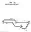
FIG. 2A is a front view of the printed wires and vias on front side 230 of a PCB (not depicted) in a DIMM (not depicted) that fall within the overlying footprint of a memory device (not depicted), according to the Background Art. FIG. 2B is a back-side view of the printed wires and vias on a back side 232 of the same PCB in the same DIMM that fall within the overlying footprint of a positional-twin memory device (not depicted), according to the Background Art. FIG. 2C is a front view of the printed wires and vias of the PCB that fall within the overlapped footprints of the positional-twin memory devices, according to the Background Art. FIGS. 2A-2C (again) are provided to help relate FIGS. 1B and 1C to FIG. 1A.
A description of how FIG. 2C is obtained can be as follows: rotate FIG. 2B 180° about a flip axis 24; and then superimpose FIG. 2A upon the rotated version of FIG. 2B. Alternatively, a description of how FIG. 2C is obtained can be as follows: make a left-hand rotation of FIG. 2A about a fold axis 26 and make a right-hand rotation of FIG. 2B about fold axis 26, bringing FIG. 2A toward FIG. 2B as one might close a book or fold a sheet of paper; and then make a right-hand rotation of the closed-book/folded-sheet until the wires in the closed-book/folded-sheet corresponding to the wires in FIG. 2A have the same orientation as in FIG. 2A.
In FIG. 2C, vias 11 and 12 connect wires 16 & 20 and 22 & 18, respectively. Pads 1a and 1b′ (or, in other words, end portions) of wires 16 and 22, respectively, are not electrically connected, but they do overlap (again, given the relationship of FIG. 2C to FIGS. 2A-2B). Hence, in FIG. 2C, one circle encloses both reference numbers 1a and 1b′. Similarly, pads 1a′ and 1b of wires 20 and 18, respectively, are not electrically connected, but they do overlap. Accordingly, in FIG. 2C, one circle encloses both reference numbers 1a′ and 1b.
Returning to FIGS. 1A-1B, conductive terminals 106 can be described as being clustered along opposing edges of each memory device 104—i. In contrast and relative to the arrangement of conductive terminals 106, vias 108—i can be described as being clustered along a central axis of each memory device 104—i.
SUMMARY OF THE PRESENT INVENTIONAn embodiment of the present invention provides an inline memory module (IMM) architecture. Such an IMM architecture may include: a printed circuit board (PCB); a first array of memory devices on a first side of the PCB; a second array of memory devices on a second side of the PCB; at least some of the memory devices of the first array being arranged so as to substantially overlap, relative to a reference axis of the PCB, positional-twin memory devices of the second array, respectively; and multiple vias at least some of which are parts of respective signal paths that connect I/O terminals of a first memory device in the first array to corresponding I/O terminals of a second memory device in the second array that is adjacent to a positional-twin third memory device in the second array corresponding to the first memory device.
BRIEF DESCRIPTION OF THE DRAWINGSFIG. 1A is a cross-section of a DIMM, according to the Background Art, taken along section line IA-IA′ shown in FIGS. 1B and 1C.
FIG. 1B is a front view of the printed wires and vias of the PCB of FIG. 1A that fall within the overlying footprints of first positional-twin memory devices thereon, according to the Background Art.
FIG. 1C is a front view of the printed wires and vias of the PCB of FIG. 1A that fall within the overlying footprints of second positional-twin memory devices thereon, according to the Background Art.
FIG. 2A is a front view of the printed wires and vias on a front side of a PCB (not depicted) in a DIMM (not depicted) that fall within the overlying footprint of an memory device (not depicted), according to the Background Art.
FIG. 2B is a rear view of the printed wires and vias on a back side of the same PCB in the same DIMM as in FIG. 2B that fall within the overlying footprint of a positional-twin memory device (not depicted), according to the Background Art.
FIG. 2C is a front view of the printed wires and vias of the PCB of FIGS. 2A & 2B that fall within the overlapped footprints of the positional-twin memory devices, according to the Background Art.
FIG. 3 is a block diagram of an in-line memory module (IMM), e.g., a dual IMM (DIMM) of any of the various varieties thereof, according to an embodiment of the present invention.
FIG. 4A is a cross-section of an IMM, e.g., a DIMM of any of the various varieties thereof, according to an embodiment of the present invention, where the section line (not depicted) is similar to the section line depicted in FIGS. 1A & 1B.
FIG. 4B is a front view of the IMM of FIG. 4A.
FIG. 4C is an exploded view of adjacent ith and (i+1)th memory devices in the IMM of FIG. 4A, according to an embodiment of the present invention.
FIG. 4D is a cross-section of an IMM, according to an embodiment of the present invention, that represents an alternative arrangement to the IMM of FIG. 4A.
FIG. 5A is a front view of the printed wires and vias on a front side of a PCB (albeit not depicted in FIG. 5A) in an IMM (albeit not depicted in FIG. 5A) with respect to the overlying footprints of memory devices i_f and i+1_f, according to an embodiment of the present invention.
FIG. 5B is a front view of the printed wires and vias on the back side of the PCB (albeit not depicted in FIG. 5A) in IMM 400 (albeit not depicted in FIG. 5A) with respect to the overlying footprints of memory devices i_r and i+1_r, according to an embodiment of the present invention.
FIG. 5C is a view of a portion of FIG. 5A superimposed on a portion of a flipped version of FIG. 5B.
FIG. 6A is a cross-section of an IMM, according to an embodiment of the present invention, where the section line (not depicted) is similar to the section line depicted in FIGS. 1A & 1B.
FIG. 6B is a front view of the IMM of FIG. 6A.
FIG. 6C is an exploded view of adjacent ith and (i+1)th devices in the IMM of FIG. 6A, according to an embodiment of the present invention.
FIG. 7A is a front view of the printed wires and vias on a front side 630 of PCB 619 (albeit not depicted in FIG. 7A) in IMM 600 (albeit not depicted in FIG. 7A) with respect to the overlying footprints of memory devices 604—i—f and 604—i+1—f, according to an embodiment of the present invention.
FIG. 7B is a front view of the printed wires and vias on back side 632 of PCB 619 (albeit not depicted in FIG. 7A) in IMM 600 (albeit not depicted in FIG. 7A) with respect to the overlying footprints of memory devices 604—i—r and 604—i+1—r, according to an embodiment of the present invention.
FIG. 7C is a view of a portion of FIG. 7A superimposed on a portion of a flipped version of FIG. 7B.
FIG. 8 is a cross-section of an IMM, according to another embodiment of the present invention, where the section line (not depicted) is similar to the section line depicted in FIGS. 1A & 1B.
FIG. 9 is a cross-section of an IMM, according to another embodiment of the present invention, where the section line (not depicted) is similar to the section line depicted in FIGS. 1A & 1B.
DETAILED DESCRIPTION OF EXAMPLE EMBODIMENTSThe present invention will be described more fully with reference to the accompanying drawings, in which example embodiments of the present invention are shown. It should be understood, however, that example embodiments of the present invention described herein can be modified in form and detail without departing from the spirit and scope of the present invention. Accordingly, the embodiments described herein are provided by way of example and not of limitation, and the scope of the present invention is not restricted to the particular embodiments described herein.
In particular, the relative thicknesses and positioning of structures or regions may be reduced or exaggerated for clarity. In other words, the figures are not drawn to scale. Further, a structure is considered as being formed “on” another structure when formed either directly on the referenced structure or formed on other structures overlaying the referenced structure.
Reference number similarities from one figure to the next may suggest at least similar components/items.
In developing embodiments of the present invention, the following observation regarding the Background Art arrangement of wires on the PCB of a DIMM was made, and a path to an alternate arrangement of wires on a PCB of an inline memory module (IMM) was identified. Clustering the vias along a central axis (see, e.g., Background Art FIGS. 1B & 1C) tends to produce combined front and rear wire lengths (LA+LB) that are longer than is desirable (due, e.g. to being proportional to device withdth), which can induce unnecessary signal propagation delays. At least one embodiment of the present invention reduces (if not substantially minimizes) wire lengths.
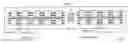
FIG. 3 is a block diagram of an in-line memory module (IMM) 300, e.g., a dual IMM (DIMM) of any of the various varieties thereof, according to an embodiment of the present invention. More particularly, the IMM 300 can be, e.g., a registered DIMM (RDIMM) such as might be used in a server, an unregistered DIMM (UDIMM) such as might be used in a PC, a small outline DIMM (SO DIMM), a micro DIMM, a double data rate DIMM (DDR DIMM), etc.
In FIG. 3, the IMM 300 includes a plurality of integrated circuit memory devices, 301, 302, . . . , 317 and 318, where each memory device can be the same. For example, integrated circuit memory devices 301, 302, . . . , 317 and 318 can be packaged devices each of which contains one or more integrated circuit chips, where the packaging may take the form, e.g., of plastic loaded packages, BGAs (ball grid arrays), WFPs (wafer-level fabricated packages), etc.
Stubs 320—k (320_01—k, . . . , 320_18—k) can connect memory devices 301-318 to transmission lines 322 and 324, respectively. Stubs 326 and 328 can connect transmission lines 322 & 324 to a bus 330. In other words, memory devices 301-310 (for each kth input/output (I/O) terminal), can be coupled to bus 330 via stub 326, transmission line 322 and stubs 320_01—k-320_10—k. Memory devices 311-318 (for each kth I/O terminal) can be coupled to bus 330 via stub 328, transmission line 324 and stubs 320_11—k-320_18—k. Different groupings of memory devices can be included in such an IMM. Other numbers of memory devices can be included in such an IMM. Other arrangements of stubs, transmission lines and/or buses can be used to implement such an IMM.
Each common input/output (I/O) terminal of memory devices 301-318 typically is functionally the same. Each common input/output (I/O) terminal of memory devices 301-318 can be connected together, respectively. Of the plurality of I/O terminals that each of memory devices 301-318 comprises, only one such I/O terminal is depicted in FIG. 3. In other words, the wires depicted in FIG. 3, namely stubs 320—k, transmission lines 322 & 324, stubs 326 & 328 and bus 330 represent a simplification by which the signal path for only one of the given common terminals of memory devices 301-318 is depicted.
Memory devices, e.g., 303 & 304 align at a first reference location (relative to a reference axis, e.g., the longitudinal axis of a PCB that is not shown in FIG. 3 but which is included in IMM 300), so as to at least significantly overlap each other. Similarly, e.g., memory devices 307 & 308 align at a second reference location so as to significantly overlap each other. To simplify description, memory devices 303 & 304 will be referred to as a positional-twin pair 332_03&04, memory devices 307 and 308 will be referred to as a positional-twin pair 332_07&08, etc.
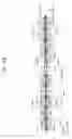
FIG. 4A is a cross-section of an IMM 400, e.g., a DIMM of any of the various varieties thereof, according to an embodiment of the present invention, where the section line (not depicted) is similar to the section line depicted in FIGS. 1A & 1B. The IMM 400 can be an example of IMM 300.
In FIG. 4A, IMM 400 includes: a printed circuit board (PCB) 419; and integrated circuit memory devices 301-318. Even numbered memory devices 302-318 represent a first array of memory devices on a first side of PCB 419. Odd numbered memory devices 301-311 represent a second array of memory devices on a second side of PCB 419. Conductive terminals 406, e.g. conductive balls, as I/O terminals of the memory devices can connect conductive I/O terminals of the circuits (not shown) in memory devices 301-318 to the various wires on PCB 419, respectively. The IMM 400 further can include integrated circuit devices 434A and 434B. Each of devices 434A & 434B can be a buffer or a register device.
Relative to a reference axis, e.g., the longitudinal axis of PCB 419, memory devices in the first array can be described as substantially completing overlapping memory devices in the second array. More specifically, e.g., memory devices 303 & 304 of IMM 400 align at a first reference location so as to substantially completely overlap each other. Similarly, e.g., memory devices 307 & 308 of IMM 400 align at a second reference location so as to substantially completely overlap each other. Among the plurality of positional-twin pairs depicted in FIG. 4A, to simplify illustration only two are called out, namely positional-twin pairs 432_03&04 432_07&08. At least some of terminals 406 for memory devices 301-318 can be described as being clustered along opposing edges of each such memory device, in a manner similar to what is depicted in FIGS. 1B & 1C.
Also in FIG. 4A (similar to FIG. 3), the cross-section is taken so that the signal path for only one set of common input/output (I/O) terminals of memory devices 301-318 are represented. Hence, the wires depicted in FIG. 4A, namely stubs 420—i—k and transmission lines 422 & 424, represent a simplification by which the signal path for only one (hereafter, the kth one) of the common terminals of memory devices 301-318 is depicted.
Even numbered stubs are depicted in FIG. 4A although only stubs 420_12—k and 420_14—k are called out, for simplicity of illustration. Similarly, odd numbered stubs also are depicted in FIG. 4A although only stubs 420_13—k and 420_15—k are called out, for simplicity of illustration.
FIG. 4B is a front view of IMM 400.
In FIG. 4B, even numbered stubs are depicted although only stubs 420_08—k and 420_14—k are called out, for simplicity of illustration. As FIG. 4B is a front view, the numbering convention for the vias reflects the footprints of the memory devices between which the via is located. For example, via 408_08&10_k should be understood as indicating that this via is located in a region between terminals 406 for memory devices 308 & 310 on the front side of PCB 419 depicted in FIG. 4B. The even numbered stubs (420_08—k, 420_14—k, etc.) can connect vias 408—m&(m+2)_k to the even numbered memory devices(302, 304, 306 . . . ), where m represents the number of a first even numbered memory device on a front side 430 (see FIG. 4C) of PCB 419, m+2 represents the number of the memory device adjacent (relative to the reference axis) to the first numbered memory device, and k reflects that FIG. 4B depicts the signal path for the kth one of the common terminals of the memory devices. For example, stubs 420_08—k and 420_16—k can connect vias 408_08&10—k and 408_14&16—k to memory devices 308 and 314, respectively.
Odd numbered stubs also are depicted in FIG. 4B although only stubs 420_09—k and 420_15—k are called out, for simplicity of illustration. It is to be understood that the odd numbered stubs are located on the other side of PCB 419 relative to the even numbered stubs, but PCB 419 has been depicted as partially transparent in order to make the odd numbered studs visible in FIG. 4B and thus better convey the relationship between the odd numbered stubs & the even numbered stubs and the vias. The odd numbered stubs (420_09—k, 420_15—k, etc.) can connect vias 408—m&(m+2)_k to the odd numbered memory devices (not shown in FIG. 4B) on the other side of PCB 419, where m can represent a given memory device on front side 430 of PCB 419, m−1 can represent the number of the positional-twin memory device (namely, an odd numbered memory device) on rear side 432 (see FIG. 4C) of PCB 419 relative to memory device m, and m−3 can represent the number of a memory device on rear side 432 adjacent (relative to the reference axis) to the positional-twin memory device. For example, stubs 420_09—k and 420_15—k can connect vias 408_8&10—k and 408_16&14—k to memory devices 309 (not shown in FIG. 4B) and 315 (not shown in FIG. 4B).
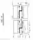
FIG. 4C is an exploded view of adjacent ith and (i+1)th devices in IMM 400, according to an embodiment of the present invention.
Inspection of FIG. 4C reveals that PCB 419 has a front side 430 and a back side 432. Memory devices 404—i—f and 404—i+1—f can be mounted on front side 430 of PCB 419. Memory devices 404—i—r and 404—i+1—r can be mounted on the back side 432 of PCB 419. Conductive segments (again, referred hereto as wires) are printed on front side 430 and the back side 432 of PCB 419. More particularly, wires 416—k, 418—k, 424—k and 426—k are visible in FIG. 4C on front side 430 of PCB 419, and wires 414—k, 421—k, 422—k and 428—k are visible in FIG. 4C on the back side 432 of PCB 419. The vias are formed in PCB 419, of which via 408—k is visible in FIG. 4C.
The via 408—k can be part of a signal path that connects wire 420—k for memory device 404—i—r to wire 426—k for memory device 404—i+1—f. It is to be observed that memory device 404—i+1—r is adjacent (in terms of the reference axis) to memory device 404—i—r, where memory device 404—i+1—r can be described as the positional-twin of memory device 404—i+1—f. As such, via 408—k can be described as being located in a region defined between terminals 406 (or the underlying portions of the wires connected thereto) of adjacent (in terms of the reference axis) memory devices 404—i—r and 404—i+1—r. That region, in terms of FIG. 4C, also happens to be defined between terminals 406 (or the overlying portions of the wires connected thereto) of adjacent (in terms of the reference axis) memory devices 404—i—f and 404—i+1—f.
In FIG. 4C, the combined length LA+LB of electrically connected wires, e.g., 420—k and 426—k, is significantly (if not substantially) shorter than corresponding wires in the central axis-clustered arrangement Background Art FIG. 1A. This is because, e.g., via 408—k is not located under a central axis of either memory devices 404—i—r or 404—i+1—f. Rather, via 408—k is located between memory devices 404i—r and 404—i+1—f so as to be closer to the pertinent conductive terminals of both of memory devices 404—i—r and 404—i+1—f, not merely one (which may be a generous description) or the other.
A fuller understanding of FIGS. 4A & 4C can be facilitated with reference to FIGS. 5A-5C.
FIG. 5A is a front view of the printed wires and vias on the front side 430 of PCB 419 (albeit not depicted in FIG. 5A) in IMM 400 (albeit not depicted in FIG. 5A) with respect to the overlying footprints of memory devices 404—i—f and 404—i+1—f, according to an embodiment of the present invention. FIG. 5B is a front view of the printed wires and vias on back side 432 of PCB 419 (albeit not depicted in FIG. 5A) in IMM 400 (albeit not depicted in FIG. 5A) with respect to the overlying footprints of memory devices 404—i—r and 404—i+1—r, according to an embodiment of the present invention. FIG. 5C is a view of a portion of FIG. 5A superimposed on a portion of a flipped version of FIG. 5B, in which the printed wires and vias of PCB 419 (albeit not depicted in FIG. 5A) in the IMM 400 (albeit not depicted in FIG. 5A) that fall within the overlapped footprints of positional-twin pairs 332—i—f&r (comprised of memory devices 404—i—f & 404—i—r) and 332—i+1—f&r (comprised of memory devices 404—i+1—f & 404—i+1—r) are depicted. FIGS. 5A-5C (again) are provided to enhance understanding of FIGS. 4A-4C.
A description of how FIG. 5C is obtained can be as follows: rotate FIG. 5B 180° about a flip axis 524; and then superimpose FIG. 5A upon the rotated version of FIG. 5B. Alternatively, a description of how FIG. 5C is obtained can be as follows: make a left-hand rotation of FIG. 5A about a fold axis 524 and make a right-hand rotation of FIG. 5B about fold axis 524, bringing FIG. 5A toward FIG. 5B as one might close a book or fold a sheet of paper; and then make a left-hand rotation of the closed-book/folded-sheet until the wires in the closed-book/folded-sheet corresponding to the wires in FIG. 5A have the same orientation as in FIG. 5A.
In FIG. 5C, vias 501 and 503 can connect wires 520 & 524 and 522 & 526, respectively. Pads 1a and 1b′ (or, in other words, end portions) of wires 522 and 524, respectively, are not electrically connected, but they do overlap (again, given the relationship of FIG. 5C to FIGS. 5A-5B). Hence, in FIG. 5C, one circle encloses both reference numbers 1a and 1b′. Similarly, pads 1a′ and 1b of wires 526 and 520, respectively, are not electrically connected, but they do overlap. Accordingly, in FIG. 5C, one circle encloses both reference numbers 1a′ and 1b.
It is to be noted that all of the statements made above apply to most of memory devices 301-318. But there can be exceptions for the outer devices 309 & 310 and 311 & 312, and for the inner devices 301 & 302 and 317 & 318. Stubs 420_12—k & 420_13—k can be considered as paired stubs. Similarly, stubs 420_14—k & 420_15—k, as well as others not explicitly called out, namely 420_16—k & 420_17—k, 420_02—k & 420_03—k, 420_04—k & 420_05—k, 420_06—k & 420_07—k and 420_08—k & 420_09—k, can be considered as paired stubs. But stubs 420_11—k, 420_18—k, 420_01—k and 420_10—k can be considered as unpaired stubs.
FIG. 4D is a cross-section of an IMM 400′, according to an embodiment of the present invention, that represents an alternative arrangement to the IMM 400 of FIG. 4A.
In IMM 400′, locations of the vias assigned to unpaired stubs 420_11′—k, 420_18′—k, 420_01′—k and 420_10′—k have been moved relative to their counterpart unpaired stubs 420_11—k, 420_18—k, 420_01—k and 42010k in FIG. 4A, respectively. More particularly, the vias have been moved inward from peripheral signal pads of the respective memory devices 311, 318, 301 and 310, respectively. Such inward locations can, e.g., reduce a length of the unpaired stubs, respectively.
Other locations of vias for the paired stubs are contemplated. For example, consider FIG. 6A.
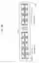
FIG. 6A is a cross-section of an IMM 600, e.g., a DIMM of any of the various varieties thereof, according to an embodiment of the present invention, where the section line (not depicted) is similar to the section line depicted in FIGS. 1A & 1B. The IMM 600 can be another example of IMM 300.
In FIG. 6A, the IMM 600 includes: a printed circuit board (PCB) 619; and integrated circuit memory devices 301-318. Even numbered memory devices 302-318 represent a first array of memory devices on a first side of PCB 619. Odd numbered memory devices 301-311 represent a second array of memory devices on a second side of PCB 619. Conductive terminals 406, e.g., conductive balls, as I/O terminals of the memory devices can connect conductive I/O terminals of the circuits (not shown) in memory devices 301-318 to the various wires on PCB 619, respectively. The IMM 600 further can include buffer or register devices 434A and 434B.
Relative to a reference axis, e.g., the longitudinal axis of PCB 619, memory devices in the first array can be described as substantially completing overlapping memory devices in the second array. More specifically, e.g., memory devices 303 & 304 of the IMM 400 align at a first reference location so as to substantially completely overlap each other. Similarly, e.g., memory devices 307 & 308 of the IMM 400 align at a second reference location so as to substantially completely overlap each other. Among the plurality of positional-twin pairs depicted in FIG. 6A, to simplify illustration only two are called out, namely positional-twin pairs 632_03&04 632_07&08. At least some of terminals 406 of memory devices 301-318 can be described as being clustered along opposing edges of each such memory device, in a manner similar to what is depicted in FIGS. 1B & 1C.
Also in FIG. 6A (similar to FIG. 3), the cross-section is taken so that signal path for only one set of common input/output (I/O) terminals of memory devices 301-318 are represented. Hence, the wires depicted in FIG. 6A, namely stubs 620—i—k and transmission lines 622 & 626, represent a simplification by which signal path for only one (hereafter, the kth one) of the common terminals of memory devices 301-318 is depicted.
Even numbered stubs are depicted in FIG. 6A although only stubs 620_12—k and 620_14—k are called out, for simplicity of illustration. Similarly, odd numbered stubs also are depicted in FIG. 6A although only stubs 620_13—k and 620_15—k are called out, for simplicity of illustration.
FIG. 6B is a front view of IMM 600.
In FIG. 6B, even numbered stubs are depicted although only stubs 620_08—k and 620_16—k are called out, for simplicity of illustration. As FIG. 6B is a front view, the numbering convention for the vias reflects the footprint of the memory device in which the via is located. For example, via 608_10—k should be understood as indicating that this via is located within the footprint of memory device 310. The even numbered stubs can connect vias 608—m—k to the even numbered memory devices, where m represents the number of the memory device on the first side of a PCB 619 depicted in FIG. 6B. For example, stubs 620_08—k and 620_16—k can connect vias 608_10—k and 608_16—k to memory devices 308 and 314, respectively.
Odd numbered stubs also are depicted in FIG. 6B although only stubs 620_09—k and 620_15—k are called out, for simplicity of illustration. It is to be understood that the odd numbered stubs are located on the other side of PCB 619 relative to the even numbered stubs, but PCB 619 has been depicted as partially transparent in order to make the odd numbered studs visible in FIG. 6B and thus better convey the relationship between the odd numbered stubs & the even numbered stubs and the vias. The odd numbered stubs can connect vias 608—m—k to the odd numbered memory devices (not shown in FIG. 6B) on the other side of PCB 619, where m represents the number of the positional-twin memory device relative thereto on the first side 630 of PCB 619. For example, stubs 620_09—k and 620_15—k can connect vias 608_10—k and 608_16—k to memory devices 309 (not shown in FIG. 6B) and 315 (not shown in FIG. 6B).
FIG. 6C is an exploded view of adjacent ith and (i+1)th devices in IMM 600, according to an embodiment of the present invention.
Inspection of FIG. 6C reveals that PCB 619 has a front side 630 and a back side 632. Memory devices 604—i—f and 604—i+1—f can be mounted on front side 630 of PCB 619. Memory devices 604—i—r and 604—i+1—r can be mounted on back side 632 of PCB 619. Conductive segments (again, referred hereto as wires) are printed on the front side 630 and the back side 632 of PCB 619. More particularly, wires 618—k, 624—k and 626—k are visible in FIG. 6C on front side 630 of PCB 619, and wires 614—k, 620—k, 622—k and 628—k are visible in FIG. 6C on back side 632 of PCB 619. The vias are formed through PCB 619, of which via 608—i—k and 608—i+1—k are visible in FIG. 6C.
The via 608—k can be part of a signal path that connects wire 620—k of memory device 604—i—r to wire 626—k for memory device 604—i+1—f. It is to be observed that memory device 604—i—f is adjacent (in terms of the reference axis) to memory device 604—i+1—f, where memory device 604—i—f can be described as the positional-twin of memory device 604—i—r. As such, via 608—i—k can be described as being located inward from peripheral terminals 406 (or the underlying portions of the wires connected thereto) of each of the positional-twin memory devices 604—i—r and 604—i—f.
In FIG. 6C, the combined length LA+LB of electrically connected wires, e.g., 620—k and 626—k is significantly (if not substantially) shorter than corresponding wires in the central axis-clustered arrangement Background Art FIG. 1A. This is primarily because of the arrangement of wire 626—k.
A fuller understanding of FIGS. 6A & 6C can be facilitated with reference to FIGS. 7A-7C.
FIG. 7A is a front view of the printed wires and vias on a front side 630 of PCB 619 (albeit not depicted in FIG. 7A) in IMM 600 (albeit not depicted in FIG. 7A) with respect to the overlying footprints of memory devices 604—i—f and 604—i+1—f, according to an embodiment of the present invention. FIG. 7B is a front view of the printed wires and vias on back side 632 of PCB 619 (albeit not depicted in FIG. 7A) in IMM 600 (albeit not depicted in FIG. 7A) with respect to the overlying footprints of memory devices 604—i—r and 604—i+1—r, according to an embodiment of the present invention.
FIG. 7C is a view of a portion of FIG. 7A superimposed on a portion of a flipped version of FIG. 7B, in which the printed wires and vias of PCB 619 (albeit not depicted in FIG. 7A) in IMM 600 (albeit not depicted in FIG. 7A) that fall within the overlapped footprints of positional-twin pairs 604—i—f&r (comprised of memory devices 604—i—f & 604—i—r) and 604—i+1—f&r (comprised of memory devices 604—i+1—f & 604—i+1—r).
FIGS. 7A-7C (again) are provided to enhance understanding of FIGS. 6A-6C. A description of how FIG. 7C is obtained can be as follows: rotate FIG. 7B 180° about a flip axis 724; and then superimpose FIG. 7A upon the rotated version of FIG. 7B.
In FIG. 7C, vias 701 and 702 can connect wires 720 & 724 and 722 & 726, respectively. Pads 1a and 1b′ (or, in other words, end portions) of wires 726 and 724, respectively, are not electrically connected, but they do overlap (again, given the relationship of FIG. 7C to FIGS. 7A-7B). Hence, in FIG. 7C, one circle encloses both reference numbers 1a and 1b′. Similarly, pads 1a′ and 1b of wires 722 and 720, respectively, are not electrically connected, but they do overlap. Accordingly, in FIG. 7C, one circle encloses both reference numbers 1a′ and 1b.
It is noted that all of the statements made above apply regarding FIGS. 6A-6C and 7A-7C apply to most of memory devices 301-318. But there can be exceptions; it is to be recalled that stubs 320_11—k, 320_18—k, 320_01k and 3201310—k of FIG. 3 can be considered as unpaired stubs; see the discussion of stubs 420_11—k, 420_18—k, 420_01—k and 420_10—k above.
In addition to vias 608—m—k discussed above, FIG. 6B also depicts an additional column 640 of vias located within the footprint of memory device 310 and an additional column 642 of vias located within the footprint of memory device 318. Column 640 includes vias 608_10′—k. Column 642 includes vias 608_18′—k. More particularly, the vias in columns 640 and 642 have been moved inward from peripheral signal pads of the respective memory devices 310 and 318, as opposed to being adjacent thereto as continuation of the pattern established relative to memory devices 302-308 and 312-316 might suggest, respectively. Such inward locations can, e.g., reduce a length of the unpaired stubs, respectively.
Other alignments between the first and second set of arrays of memory devices on the opposite sides of PCB are contemplated. For example, consider FIG. 8.
FIG. 8 is a cross-section of an IMM 800, e.g., a DIMM of any of the various varieties thereof, according to an embodiment of the present invention, where the section line (not depicted) is similar to the section line depicted in FIGS. 1A & 1B. The IMM 800 can be an example of IMM 300.
FIG. 8 is similar in many respects to FIGS. 4A-4C. The IMM 800 can be, e.g., a DIMM of any of the various varieties thereof.
In FIG. 8, IMM 800 includes: a printed circuit board (PCB) 819; and integrated circuit memory devices 301-318. Even numbered memory devices 302-318 represent a first array of memory devices on a first side of PCB 819. Odd numbered memory devices 301-311 represent a second array of memory devices on a second side of PCB 819. Conductive terminals 406 e.g., conductive balls, as I/O terminals of the memory devices can connect conductive I/O terminals of the circuits (not shown) in memory devices 301-318 to the various wires on PCB 819, respectively. The IMM 800 further can include buffer or register devices 434A and 434B.
Relative to a reference axis, e.g., the longitudinal axis of PCB 819, the memory devices in the first array can be described as significantly displaced or shifted relative to the memory devices in the second array, as indicated by the arrow in phantom lines called out by reference number 850. Despite being shifted, however, the memory devices in the first array can be described as substantially overlapping the memory devices in the second array. More specifically, e.g., memory devices 303 & 304 of IMM 800 substantially align relative to a first reference location and yet, e.g., memory device 304 is displaced relative to the first reference location. Similarly, e.g., memory devices 307 & 308 of IMM 800 substantially align relative to a second reference location and yet, e.g., memory device 308 is displaced relative to the second reference location.
Among the plurality of positional-twin pairs depicted in FIG. 8, only two (for the purpose of simplifying illustration) are called out, namely positional-twin pairs 832_03&04 and 832_07&08. Positional twin pair 832_07&08 includes memory devices 307 and 308. Similarly, positional twin pair 832_03&04 includes memory devices 303 and 304. In FIG. 8, at least some of terminals 406 for memory devices 301-318 can be described as being clustered along opposing edges of each such memory device, in a manner similar to what is depicted in FIGS. 1B & 1C.
Also in FIG. 8 (similar to FIG. 3), the cross-section is taken so that the signal path for only one set of common input/output I/O terminals of memory devices 301-318 are represented. Hence, the wires depicted in FIG. 8, namely stubs 820—i—k and transmission lines 822 & 824, represent a simplification by which the signal path for only one (hereafter, the kth one) of the common terminals of memory devices 301-318 is depicted.
Even numbered stubs are depicted in FIG. 8 although only stubs 820_12—k and 820_14—k are called out, for simplicity of illustration. Similarly, odd numbered stubs also are depicted in FIG. 8 although only stubs 820_13—k and 820_15—k are called out, for simplicity of illustration.
The vias 852—m&m+1—k can be part of a signal path that connects a wire for an mth memory device to a wire for an m+1th memory device. In FIG. 8, the numbering convention for the vias reflects that the vias form a part of the signal path between memory device m and memory device m+1.
Consider, for example, memory devices 306-308 in FIG. 8. The via 852_6&7—k is a part of the signal path that connects a wire for memory device 306 and a wire for memory device 307. It is to be observed that memory device 305 is adjacent (in terms of the reference axis) to memory device 307. The location of via 852_6&7—k can be described as being located in a region defined between terminals 406 (or the underlying portions of the wires connected thereto) of adjacent (in terms of the reference axis) memory devices 307 and 305. That region, in terms of FIG. 8, also can be described in terms of memory devices 307 and 308, namely as being located inward from peripheral terminals 406 (or the underlying portions of the wires connected thereto) of memory device 308 and yet as still being outward of peripheral terminals 406 (or the underlying portions of the wires connected thereto) of memory device 307. It is noted that memory device 308 itself can be described as the positional-twin of memory device 307. Similarly, via 852_17&16—k is a part of the signal path that connects a wire for memory device 317 and a wire for memory device 316.
Alternatively, locations of vias assigned to unpaired stubs in FIG. 8 can be relocated similarly to what is depicted in FIG. 4D (relative to FIGS. 4A-4C).
FIG. 9 is a cross-section of an IMM 900, according to an embodiment of the present invention, where the section line (not depicted) is similar to the section line depicted in FIGS. 1A & 1B. The IMM 900 can be an example of IMM 300.
FIG. 9 is similar in many respects to FIGS. 6A-6C. The IMM 900 can be, e.g., a DIMM of any of the various varieties thereof.
In FIG. 9, IMM 900 includes: a printed circuit board (PCB) 919; and integrated circuit memory devices 301-318. Even numbered memory devices 302-318 represent a first array of memory devices on a first side of PCB 919. Odd numbered memory devices 301-311 represent a second array of memory devices on a second side of PCB 919. Conductive terminals 406 e.g., conductive balls, as I/O terminals of the memory devices can connect I/O terminals of the circuits (not shown) in memory devices 301-318 to the various wires on PCB 919, respectively. The IMM 900 further can include buffer or register devices 434A and 434B.
Relative to a reference axis, e.g., the longitudinal axis of PCB 919, the memory devices in the first array can be described as significantly displaced or shifted relative to the memory devices in the second array, as indicated by the arrow in phantom lines called out by reference number 950. Despite being shifted, however, the memory devices in the first array can be described as substantially overlapping the memory devices in the second array. More specifically, e.g., memory devices 303 & 304 of IMM 900 substantially align relative to a first reference location and yet, e.g., memory device 304 is displaced relative to the first reference location. Similarly, e.g., memory devices 307 & 308 of IMM 900 substantially align relative to a second reference location and yet, e.g., memory device 308 is displaced relative to the second reference location.
Among the plurality of positional-twin pairs depicted in FIG. 9, only two (for the purpose of simplifying illustration) are called out, namely positional-twin pairs 932_03&04 and 932_07&08. Positional twin pair 932_07&08 includes memory devices 307 and 308. Similarly, positional twin pair 932_03&04 includes memory devices 303 and 304. In FIG. 9, at least some of terminals 406 for memory devices 301-318 can be described as being clustered along opposing edges of each such memory device, in a manner similar to what is depicted in FIGS. 1B & 1C.
Also in FIG. 9 (similar to FIG. 3), the cross-section is taken so that only one set of common input/output I/O terminals of memory devices 301-318 are represented. Hence, the wires depicted in FIG. 9, namely stubs 920—i—k and transmission lines 922 & 924, represent a simplification by which only one (hereafter, the kth one) of the common terminals of memory devices 301-318 is depicted.
Even numbered stubs are depicted in FIG. 9 although only stubs 920_12—k and 920_14—k are called out, for simplicity of illustration. Similarly, odd numbered stubs also are depicted in FIG. 9 although only stubs 920_13—k and 920_15—k are called out, for simplicity of illustration.
The vias 952—m&m+1_k can be part of a signal path that connects a wire for an mth memory device to a wire for an m+1th memory device. In FIG. 9, the numbering convention for the vias reflects that the vias form a part of the signal path between memory device m and memory device m+1.
Consider, for example, memory devices 306-308 in FIG. 9. The via 952_6&7—k is a part of the signal path that connects a wire for memory device 306 and a wire for memory device 307. It is to be observed that memory device 305 is adjacent (in terms of the reference axis) to memory device 307. It is noted that memory device 308 itself can be described as the positional-twin of memory device 307. Similarly, via 952_17&16—k is a part of the signal path that connects a wire for memory device 317 and a wire for memory device 316.
The location of via 952_6&7—k can be described as being located inward from peripheral terminals 406 (or the underlying portions of the wires connected thereto) of memory device 307. The location of via 952_6&7—k further can be described as being located in a region defined between terminals 406 (or the overlying portions of the wires connected thereto) of adjacent (in terms of the reference axis) memory devices 308 and 306.
Embodiments of the present invention having been thus described, it will be obvious that the same may be varied in many ways. Such variations are not to be regarded as a departure from the spirit and scope of the present invention, and all such modifications are intended to be included within the scope of the present invention.
Claims
What is claimed is:1. An inline memory module (IMM) architecture comprising:
a printed circuit board (PCB);
a first array of memory devices on a first side of the PCB;
a second array of memory devices on a second side of the PCB;
at least some of the memory devices of the first array being arranged so as to substantially overlap, relative to a reference axis of the PCB, positional-twin memory devices of the second array, respectively; and
a plurality of vias at least some of which are parts of respective signal paths that connect I/O terminals of a first memory device in the first array to corresponding I/O terminals of a second memory device in the second array that is adjacent to a positional-twin third memory device in the second array corresponding to the first memory device.
2. The IMM architecture of claim 1, wherein:
at least some I/O terminals of each memory device are clustered along opposing edges of the memory device; and
locations for a majority of the vias are in regions defined between I/O terminals at edges of adjacent memory devices of the first array, respectively.
3. The IMM architecture of claim 2, wherein the regions also are defined as being between signal pads at edges of adjacent memory devices of the second array.
4. The IMM architecture of claim 2, wherein the following is true for the majority of the vias:
the via is aligned within an area inward from peripheral signal pads of the respective second memory device in the second array.
5. The IMM architecture of claim 2, wherein the adjacent memory devices are considered adjacent relative to the reference axis.
6. The IMM architecture of claim 5, wherein the longitudinal axis of the PCB is the reference axis.
7. The IMM architecture of claim 1, wherein:
at least some signal pads of each memory device are clustered along opposing edges of the memory device; and
the first array is arranged relative to the second array so that any fourth memory device in the first array is displaced, relative to the reference axis, from a corresponding positional-twin fifth memory device in the second array such that signal pads at one edge of the fifth memory device align with a region located aside signal pads at one edge of the fourth memory device.
8. The IMM architecture of claim 7, wherein the following is true for a majority of the vias:
the region is defined between the signal pads at the one edge of the fourth memory device and signal pads at one edge of a sixth memory device in the first array that is adjacent to the fourth memory device.
9. The IMM architecture of claim 1, wherein the following is true for a majority of the memory devices in the first and second arrays:
the first array is arranged relative to the second array so that any fourth memory device in the first array is displaced, relative to the reference axis, from a corresponding positional-twin fifth memory device in the second array such that the fifth memory device partially overlaps a sixth memory device in the first array that is adjacent to the fourth memory device.
10. The IMM architecture of claim 1, wherein the following is true for a majority of the vias:
the vias are located, relative to the reference axis, inward from peripheral signal pads of the memory devices of the first array, respectively.
11. The IMM architecture of claim 10, wherein:
the first array is arranged relative to the second array so that any fourth memory device in the first array is displaced, relative to the reference axis, from a corresponding positional-twin fifth memory device in the second array such that a sixth memory device in the second array adjacent to the fifth memory device partially overlaps the fourth memory device in the first array.
12. The IMM architecture of claim 10, wherein the following is true for a majority of the vias:
the vias are located, relative to the reference axis, inward from peripheral signal pads of the memory devices of the second array, respectively.
13. The IMM architecture of claim 10, wherein the following is true for a majority of the vias:
the via is aligned with an area defined between signal pads at edges of the second and third memory devices in the second array.
14. The IMM architecture of claim 1, wherein the IMM architecture is a type of dual IMM (DIMM) architecture.
15. The IMM architecture of claim 1, wherein the following is true for a majority of the vias:
the signal lead of the first memory device, for a given signal path that includes a given via, is substantially the same length as the signal lead of the second memory device.
16. An inline memory module (IMM) architecture comprising:
printed circuit board (PCB) means;
a first array of memory devices on a first side of the PCB means;
a second array of memory devices on a second side of the PCB means;
at least some of the memory devices of the first array being arranged so as to substantially overlap, relative to a reference axis of the PCB means, positional-twin memory devices of the second array, respectively; and
a plurality of via means at least some of which each via means are for connecting signal leads of a first memory device in the first array to corresponding signal leads of a second memory device in the second array that is adjacent to a positional-twin third memory device in the second array corresponding to the first memory device, respectively.
17. The IMM architecture of claim 16, wherein:
at least some signal pads of each memory device are clustered along opposing edges of the memory device; and
locations for a majority of the via means are in regions defined between signal pads at edges of adjacent memory devices of the first array, respectively.
18. The IMM architecture of claim 16, wherein the adjacent memory devices are considered adjacent relative to the longitudinal axis of the PCB means.
19. The IMM architecture of claim 16, wherein:
at least some signal pads of each memory device are clustered along opposing edges of the memory device; and
the first array is arranged relative to the second array so that any fourth memory device in the first array is displaced, relative to the reference axis, from a corresponding positional-twin fifth memory device in the second array such that signal pads at one edge of the fifth memory device align with a region located aside signal pads at one edge of the fourth memory device.
20. The IMM architecture of claim 16, wherein the following is true for a majority of the memory devices in the first and second arrays:
the first array is arranged relative to the second array so that any fourth memory device in the first array is displaced, relative to the reference axis, from a corresponding positional-twin fifth memory device in the second array such that the fifth memory device partially overlaps a sixth memory device in the first array that is adjacent to the fourth memory device.
Images & Drawings included:


Sources:
- United States Patent and Trademark Office - verify current appl. status at the USPTO↗
Recent applications in this class:
- » 20250294683 2025-09-18
CIRCUIT BOARD - » 20250294682 2025-09-18
SEMICONDUCTOR PACKAGE DEVICE AND METHOD OF MANUFACTURING THE SAME - » 20250287506 2025-09-11
ELECTRONIC DEVICE AND ELECTRONIC APPARATUS - » 20250287505 2025-09-11
SEMICONDUCTOR MODULE - » 20250280499 2025-09-04
METHODS AND APPARATUS TO CONNECT A SEMICONDUCTOR PACKAGE TO A CIRCUIT BOARD - » 20250275062 2025-08-28
PRINTED CIRCUIT BOARD - » 20250275061 2025-08-28
ELECTRONIC CIRCUIT DEVICE HAVING CLOSED-CORE INDUCTORS IN SIDE-BY-SIDE RELATION AND ASSOCIATED METHODS - » 20250267794 2025-08-21
RE-WORKABLE SOCKETED SPACE SAVING MAGNETICS - » 20250261313 2025-08-14
SEMICONDUCTOR DEVICE AND MANUFACTURING METHOD OF SEMICONDUCTOR DEVICE - » 20250261312 2025-08-14
PLACEMENT OF POWER SWITCHING DEVICES ON THROUGH HOLES VIA PADS
Recent applications for this Assignee:
- » 20250291489 2025-09-18
MEMORY DEVICE, MEMORY CONTROL DEVICE AND OPERATING METHOD OF MEMORY DEVICE FOR CHECKING COMMAND AND ADDRESS (CA) SIGNAL WITH PREDETERMINED PATTERN OF COMMAND - » 20250273015 2025-08-28
ELECTRONIC DEVICE GUIDING USER TOUCH INPUT AND METHOD FOR CONTROLLING THE SAME - » 20250265676 2025-08-21
ELECTRONIC APPARATUS AND CONTROLLING METHOD THEREOF - » 20250239461 2025-07-24
ETCHING GAS MIXTURE AND METHOD OF MANUFACTURING INTEGRATED CIRCUIT DEVICE USING THE SAME - » 20250199742 2025-06-19
ELECTRONIC DEVICE AND METHOD FOR CONTROLLING DISPLAY OF AT LEAST ONE EXTERNAL OBJECT AMONG ONE OR MORE EXTERNAL OBJECTS - » 20250199359 2025-06-19
CONNECTOR, PRINTED CIRCUIT BOARD MOUNTING THE CONNECTOR, AND DISPLAY APPARATUS INCLUDING THE SAME - » 20250174585 2025-05-29
SEMICONDUCTOR DIE AND SEMICONDUCTOR PACKAGE INCLUDING THE SAME - » 20250125179 2025-04-17
MICRO-SEMICONDUCTOR CHIP WETTING ALIGNMENT APPARATUS - » 20250103556 2025-03-27
FILE PROCESSING METHOD, ELECTRONIC APPARATUS AND STORAGE MEDIUM - » 20250069239 2025-02-27
ELECTRONIC DEVICE, METHOD, AND STORAGE MEDIUM FOR OBTAINING IMAGE FOR TRACKING