Ballast for light emitting device
US20060232179A1
2006-10-19
11/107,267
2005-04-18
✅ Patent granted
US 7,586,247 B2
2009-09-08
-
-
Joseph L Williams | Elmito Breval
2026-03-08
Abstract:
A thin resistive layer is connected in series and integrated with a light emitting device as a ballast to stabilize the current through the light emitting device.
Interested in similar patents?
Get notified when new applications in this technology area are published.
Classification:
H01L25/167 » CPC main
Assemblies consisting of a plurality of individual semiconductor or other solid state devices ; Multistep manufacturing processes thereof the devices being of types provided for in two or more different main groups of - , e.g. forming hybrid circuits comprising optoelectronic devices, e.g. LED, photodiodes
H01L33/02 » CPC further
Semiconductor devices with at least one potential-jump barrier or surface barrier specially adapted for light emission; Processes or apparatus specially adapted for the manufacture or treatment thereof or of parts thereof; Details thereof characterised by the semiconductor bodies
H01L2224/73265 » CPC further
Indexing scheme for arrangements for connecting or disconnecting semiconductor or solid-state bodies and methods related thereto as covered by; Means for bonding being of different types provided for in two or more of groups; Location after the connecting process on different surfaces Layer and wire connectors
H01L2924/00014 » CPC further
Indexing scheme for arrangements or methods for connecting or disconnecting semiconductor or solid-state bodies as covered by; Technical content checked by a classifier the subject-matter covered by the group, the symbol of which is combined with the symbol of this group, being disclosed without further technical details
H01J1/00 IPC
Details of electrodes, of magnetic control means, of screens, or of the mounting or spacing thereof, common to two or more basic types of discharge tubes or lamps
Description
BACKGROUND OF THE INVETNION1. Field of the Invention
This invention relates to light emitting device, particularly to a ballast resistor for stabilizing the current through a light emitting device.
2. Brief Description of Related Art
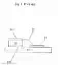
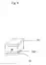
FIG. 1 shows a prior art light emitting device 10 with no current limiting resistance. If the current flowing the light emitting device is excessive, a resistor 12 should be inserted in series to limit the power consumption within a specified tolerance. In FIG. 1, the limiting resistor 12 is mounted on the same substrate 15 as the light emitting device 10 and is wire bonded to the top electrode 101 of the light emitting device 10 with its bottom electrode 102 resting over the substrate 15 through a thin metal pad over the substrate 15.
Furthermore, due to production variations, there is a distribution of the current through the light emitting device 10. In the middle of the distribution, the majority of the device satisfies the specification. Some devices lying to the left side of the distribution curve have inadequate current to satisfy the specification. Other devices lying on the right side of the distribution curve have excessive current to satisfy the specification. Either inadequate or excessive current reduces the production yield. In production, the light emitting devices must be sorted out to categorize them. Those with excessive currents have shorter life due to burnt-out, and must be sold at lower price or discarded.
In the prior art FIG. 1, a separate ballast resistor 12 is wire-bonded to the light emitting device to ballast the current. However, the separate ballast requires an extra wire bonding step and occupies extra area.
SUMMARY OF THE INVENTIONAn object of this invention of to limit the current through a light emitting device within certain limits. Another object of the present invention is to fabricate a ballast resistor without wire bonding. Still another object of the invention is to minimize the area occupied by the ballast resistor.
These objects are achieved by fabricating a ballast resistor integrally with the light emitting device. A thin layer of resistive material is connected in series with the light emitting device. The ballast layer can be either deposited over the top electrode of the light emitting device or deposited under the bottom of the light emitting device
BRIEF DESCRIPTION OF THE DRAWINGSFIG. 1 shows a prior art to connect a ballast resistor in series with a light emitting device.
FIG. 2 shows a first embodiment of the present invention with a thin film ballast layer over the top electrode of the light emitting device.
FIG. 3 shows a second embodiment of the present invention including a sealing glue between the top electrode and the ballast layer.
FIG. 4 shows a third embodiment of the present invention with a ballast layer under the bottom electrode of the light emitting device.
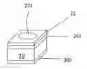
DETAILED DESCRIPTION OF THE INVENTIONFIG. 2 shows a basic structure of the present invention. A light emitting device 20 is sandwiched between a top electrode 201 and a bottom electrode 202. A thin resistive layer 22 is deposited over the top electrode 201. The resistive layer 22 has a window 221 to allow the transmission of light generated from the light emitting device 20. The lead for the top electrode 201 is attached to the thin resistive layer 22. Since this resistive layer 22 is connected in series with the light emitting device 20, it serves as a ballast to stabilize the current through the light emitting device 20. Furthermore, since the thin layer 22 is integrated with the light emitting device, no extra bonding wire is needed for external connection, and the volume occupied by the structure is minimized.
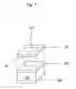
FIG. 3 shows a second embodiment of the present invention. The structure is similar to that in FIG. 2, except that a sealing glue 24 is used to modify the emitted light to focus, be parallel, or diverse. The window 221 of the resistive layer 22 can fit in the sealing glue 24. Other elements correspond to the elements in FIG. 2 with the same reference numerals.
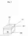
FIG. 4 shows a third embodiment of the present invention. The structure is similar to that in FIG. 2 except that the resistive layer 22 is placed at the bottom of the bottom electrode 202, which is attached to an external lead (not shown). The resistive layer 22 is connected in series with the bottom electrode 202 of the light emitting device 20 and serving as an extension end of the bottom electrode 202. It serves the same current limiting function as in FIG. 2. Other elements correspond to the elements in FIG. 2 with the same reference numerals.
While the preferred embodiments of the invention have been described, it will be apparent to those skilled in the art that various modifications can be made in the embodiments without departing from the spirit of the invention. Such modifications are all within the scope of the invention.
Claims
1. An integrated light emitting structure, comprising:
a light emitting device having a top electrode and a bottom electrode; and
a resistive layer deposited on one of said top electrode and bottom electrode as a ballast resistance to stabilize the current in said light emitting device.
2. The integrated light emitting structure as described in claim 1, wherein said resistive layer is deposited over said top electrode.
3. The integrated light emitting structure as described in claim 2, wherein said resistive layer has a window to allow transmission of light from said light emitting device.
4. The integrated light emitting structure as described in claim 3, further comprising a glue to modify the emitted light.
5. The integrated light emitting structure as described in claim 1, wherein said resistive layer is attached to the bottom of said bottom electrode.
Images & Drawings included:
Sources:
- United States Patent and Trademark Office - verify current appl. status at the USPTO↗
Similar patent applications:
Recent applications in this class:
- » 20250293223 2025-09-18
ELECTRONIC PACKAGE AND MANUFACTURING METHOD THEREOF - » 20250293222 2025-09-18
SEMICONDUCTOR DEVICES AND METHODS OF MANUFACTURE - » 20250286035 2025-09-11
ELECTRONIC DEVICE - » 20250286034 2025-09-11
DISPLAY PANEL - » 20250286033 2025-09-11
DISPLAY PANEL AND DISPLAY DEVICE - » 20250286032 2025-09-11
DISPLAY PANEL AND DISPLAY DEVICE - » 20250279403 2025-09-04
ARRAY SUBSTRATE, LIGHT-EMITTING SUBSTRATE AND DISPLAY DEVICE - » 20250279402 2025-09-04
OPTOELECTRONIC DEVICE INCLUDING A LIGHT-EMITTING DIODE STACKED ON A PHOTODETECTOR - » 20250273643 2025-08-28
DEVICE INCLUDING A PATTERNED CONDUCTIVE COATING - » 20250273642 2025-08-28
DISPLAY DEVICE