Semiconductor device structure for reducing hot carrier effect of MOS transistor
US20060246715A1
2006-11-02
10/908,071
2005-04-27
✅ Patent granted
US 7,602,003 B2
2009-10-13
-
-
Walter L Lindsay, Jr.
2026-05-05
Abstract:
A semiconductor device structure is described, including a MOS transistor, a silicon-rich silicon nitride layer having a refractive index of about 2.00-2.30, and a dielectric layer. The silicon-rich silicon nitride layer is disposed between the MOS transistor and the dielectric layer, and covers the source/drain region, the spacer and the gate conductor of the MOS transistor.
Inventors:
- Ching-Hsing Hsieh 9 🇹🇼 Hsinchu County, Taiwan
- Min-Hsian Chen 4 🇹🇼 Hsinchu County, Taiwan
- Min-Hsian Chen 1 🇹🇼 Jhudong Township, Hsinchu County, Taiwan
- Ching-Hsing Hsieh 1 🇹🇼 Jhubei, Taiwan
Assignee:
- UNITED MICROELECTRONICS CORP. 1,463 🇹🇼 Hsinchu, Taiwan
Interested in similar patents?
Get notified when new applications in this technology area are published.
Classification:
H01L29/78 IPC
Semiconductor devices adapted for rectifying, amplifying, oscillating or switching, or capacitors or resistors with at least one potential-jump barrier or surface barrier, e.g. PN junction depletion layer or carrier concentration layer; Details of semiconductor bodies or of electrodes thereof; Multistep manufacturing processes therefor; Types of semiconductor device ; Multistep manufacturing processes therefor controllable by only the electric current supplied, or only the electric potential applied, to an electrode which does not carry the current to be rectified, amplified or switched; Unipolar devices, e.g. field effect transistors; Field effect transistors with field effect produced by an insulated gate
H01L29/94 IPC
Semiconductor devices adapted for rectifying, amplifying, oscillating or switching, or capacitors or resistors with at least one potential-jump barrier or surface barrier, e.g. PN junction depletion layer or carrier concentration layer; Details of semiconductor bodies or of electrodes thereof; Multistep manufacturing processes therefor; Types of semiconductor device ; Multistep manufacturing processes therefor controllable only by variation of the electric current supplied, or only the electric potential applied, to one or more of the electrodes carrying the current to be rectified, amplified, oscillated or switched; Capacitors with potential-jump barrier or surface barrier Metal-insulator-semiconductors, e.g. MOS
H01L29/7833 » CPC further
Semiconductor devices adapted for rectifying, amplifying, oscillating or switching, or capacitors or resistors with at least one potential-jump barrier or surface barrier, e.g. PN junction depletion layer or carrier concentration layer; Details of semiconductor bodies or of electrodes thereof; Multistep manufacturing processes therefor; Types of semiconductor device ; Multistep manufacturing processes therefor controllable by only the electric current supplied, or only the electric potential applied, to an electrode which does not carry the current to be rectified, amplified or switched; Unipolar devices, e.g. field effect transistors; Field effect transistors with field effect produced by an insulated gate with lightly doped drain or source extension, e.g. LDD MOSFET's; DDD MOSFET's
H01L21/4763 IPC
Processes or apparatus adapted for the manufacture or treatment of semiconductor or solid state devices or of parts thereof; Manufacture or treatment of semiconductor devices or of parts thereof the devices having at least one potential-jump barrier or surface barrier, e.g. PN junction, depletion layer or carrier concentration layer the devices having semiconductor bodies not provided for in groups, , , and with or without impurities, e.g. doping materials; Treatment of semiconductor bodies using processes or apparatus not provided for in groups to change their surface-physical characteristics or shape, e.g. etching, polishing, cutting Deposition of non-insulating, e.g. conductive -, resistive -, layers on insulating layers; After-treatment of these layers
H01L29/76 IPC
Semiconductor devices adapted for rectifying, amplifying, oscillating or switching, or capacitors or resistors with at least one potential-jump barrier or surface barrier, e.g. PN junction depletion layer or carrier concentration layer; Details of semiconductor bodies or of electrodes thereof; Multistep manufacturing processes therefor; Types of semiconductor device ; Multistep manufacturing processes therefor controllable by only the electric current supplied, or only the electric potential applied, to an electrode which does not carry the current to be rectified, amplified or switched Unipolar devices, e.g. field effect transistors
H01L31/00 IPC
Semiconductor devices sensitive to infra-red radiation, light, electromagnetic radiation of shorter wavelength or corpuscular radiation and specially adapted either for the conversion of the energy of such radiation into electrical energy or for the control of electrical energy by such radiation; Processes or apparatus specially adapted for the manufacture or treatment thereof or of parts thereof; Details thereof
Description
BACKGROUND OF THE INVENTION1. Field of the Invention
The present invention relates to a semiconductor device structure. More particularly, the present invention relates to a semiconductor device structure capable of reducing the hot carrier effect and a method for reducing the hot carrier effect of a metal-oxide-semiconductor (MOS) transistor.
2. Description of the Related Art
MOS transistors are the most important elements in various electronic products. To compactify the electronic products, the dimensions of a MOS transistor have to be reduced. However, such a dimension reduction causes a hot carrier effect affecting the operation of the transistor. More specifically, when the channel length is decreased but the voltage applied is fixed, not only the operation speed of the transistor is increased, but also the lateral electric field in the channel is increased. Thereby, the energy of the channel electrons is increased, while the channel electrons near the drain region can be accelerated to have energy higher than the band gap of the semiconductor.
Therefore, after colliding with the valence-band electrons, the channel electrons near the drain region easily excite the valence-band electrons thereat to the conductive band to form hot electrons. A part of the hot electrons will enter the gate dielectric to cause damages, so that the reliability and the lifetime of the device are reduced.
SUMMARY OF THE INVENTIONAccordingly, one object of this invention is to provide a semiconductor device structure, which is capable of reducing the hat carrier effect to increase the lifetime of the device.
Another object of this invention is to provide a method for reducing the hot carrier effect of a MOS transistor, so as to increase the lifetime of the device.
The semiconductor device structure of this invention includes a MOS transistor, a silicon-rich silicon nitride layer having a refractive index of about 2.00-2.30, and a dielectric layer. The silicon-rich silicon nitride layer is disposed between the MOS transistor and the dielectric layer, and covers the source/drain regions, the spacer and the gate conductor of the MOS transistor.
According to some embodiments of this invention, the refractive index of the silicon-rich silicon nitride layer may be 2.0-2.05, 2.05-2.10, 2.10-2.15, 2.15-2.20, 2.20-2.25, or 2.25-2.30.
The above semiconductor device structure may further include a metal salicide layer, which is disposed on the source/drain region and the gate conductor and covered by the silicon-rich silicon nitride layer. The material of the metal salicide layer may be selected from the group consisting of nickel silicide, cobalt silicide and titanium silicide, or from nickel alloy silicides, such as nickel platinum silicide, nickel cobalt silicide and nickel titanium silicide.
In addition, the silicon-rich silicon nitride layer in the semiconductor device structure may be a tensile layer that causes a positive stress.
The method for reducing the hot carrier effect of a MOS transistor includes forming a dielectric layer with a refractive index of about 2.00-2.30 over the MOS transistor, wherein the dielectric layer covers the S/D region, the spacer and the gate conductor of the MOS transistor.
According to a preferred embodiment of this invention, the above dielectric layer may include a Si-rich SiN layer. The refractive index of the Si-rich SiN layer may be 2.0-2.05, 2.05-2.10, 2.10-2.15, 2.15-2.20, 2.20-2.25, or 2.25-2.30.
By covering the MOS transistor with a Si-rich SiN layer with a refractive index of about 2.00-2.30, the hot carrier effect is reduced to increase the lifetime of the device.
It is to be understood that both the foregoing general description and the following detailed description are exemplary, and are intended to provide further explanation of the invention as claimed.
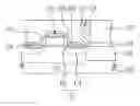
BRIEF DESCRIPTION OF THE DRAWINGSFIG. 1 illustrates a semiconductor device structure according to a preferred embodiment of this invention.
DESCRIPTION OF THE PREFERRED EMBODIMENTSReferring to FIG. 1, an isolation structure 101 is formed on a semiconductor substrate 100 to define an active area 102. A MOS transistor 104 is then formed on the substrate 100, including gate dielectric 106, a gate conductor 108, a spacer 112 and a source/drain region 115 that includes lightly and heavily doped regions 110 and 114. The MOS transistor 104 may be formed by, for example, forming a dielectric layer and a conductive layer and patterning them into the gate dielectric 106 and gate conductor 108, respectively, forming lightly doped regions 110 in the substrate 100 through ion implantation, forming a spacer 112 on the sidewall of the gate conductor 108, and then performing another implantation to form the heavily doped regions 114. The gate conductor 108 may include poly-Si, and its linewidth may be 90 nm or smaller. The gate dielectric 106 may include silicon oxide, and may have a thickness of 8-20 Å.
In another example, the MOS transistor 104 further includes a metal salicide layer 116 that is disposed on the heavily doped regions 114 and the gate conductor 108. The material of the metal salicide layer 116 may be nickel silicide, cobalt silicide or titanium silicide, or a nickel alloy silicide that is a silicide of an alloy of nickel and a refractory metal like platinum (Pt), cobalt (Co) or titanium (Ti).
Thereafter, a dielectric layer 118 with a refractive index (RI) of about 2.00-2.30 is formed over the substrate 100, the dielectric layer 118 possibly being a Si-rich SiN layer that is formed as a tensile layer. In some cases, the RI of the Si-rich SiN layer is 2.00-2.05. In other cases, the RI of the SiN layer may be 2.05-2.10, 2.10-2.15, 2.15-2.20, 2.20-2.25, or 2.25-2.30.
The Si-rich SiN layer may be formed with the following methods, for example. In some examples using a CVD chamber equipped with a high-frequency (HF) power and a low-frequency (LF) power, the carrier gas may be N2, the reaction gases may be SiH4 and NH3, and the LF power is lowered, for example, from ordinary 400W to about 0W, to reduce the bombardments of charged species to the substrate. It is also feasible to lower the HF and LF powers at the same time. For example, the HF power may be lowered from ordinary 600W to 100W and the LF power from ordinary 400W to about 0W to reduce the bombardments of charged species to the substrate. In other examples using a chamber with a single power source, the power can be lowered from ordinary 450W to 100-250W to decrease the decomposition rate of the reaction species.
Alternatively, N2 is used as a carrier gas, SiH4 is introduced in a flow rate of about 60 sccm, and the flow rate of NH3 is lowered from ordinary 30 sccm or even set as 0 to reduce the nitrogen content in the deposited silicon nitride layer. It is also feasible to lower the power and decrease the flow rate of NH3 simultaneously.
After the dielectric layer 118 is formed, another dielectric layer 120 is formed thereon, possibly including silicon oxide or a low-k material. Then, the dielectric layer 120 is etched using a patterned photoresist layer (not shown) as an etching mask to form a contact opening 122 exposing a portion of the dielectric layer 118, which serves as an etching stop layer and is then removed for electrical connection. After the photoresist layer is removed, a conductive material like aluminum (Al) or tungsten (W) is filled into the contact opening 122 to form a contact 124.
EXAMPLESExamples A1-A2 and B1-B3 use an A-type chamber and a B-type chamber, respectively. The deposition parameters and the experiment result of each example are listed in Table 1.
| TABLE 1 | |
| Example |
| A1 | B1 | B2 | |
| Recipe | HF (W) | 600 W | 170 W | 100 W |
| LF (W) | 0 | 150 W | 0 | |
| SH4 (sccm) | 500 | 60 | 160 | |
| NH3 (sccm) | 4000 | 0 | 600 | |
| N2 (sccm) | 1600 | 3000 | 600 | |
| Properties | Refractive index | 2.22 | 2.05 | 2.2 |
| of film | Si—H (/cm3) | 1.9 × 10²² | 6.2 × 10²¹ | 1.8 × 10²² |
| HCl (year) | 219 | 120 | 379 | |
As indicated by Example A1, by turning off the LF power, the Si-rich SiN layer obtained has a higher silicon content and a higher refractive index. The hot carrier injection (HCl) index of the device obtained from Example A1 is 219 years.
Moreover, as indicated by Examples B1 and B2, the Si-rich SiN layer obtained from Example B2, in which the HF and LF powers are lowered at the same time, has a higher silicon content and a higher refractive index. By lowering the HF and LF powers at the same time in the SiN deposition, the HCl index of the device obtained from Example B2 is increased from 120 years to 379 years.
When the SiN layer formed over the MOS transistor has a refractive of merely 1.95, the HCl index of the device is merely about 10 years. However, according to the above experiment results, by forming a Si-rich SiN layer with a higher refractive index, the HCl index can be much increased by several times or even tens of times. Hence, the semiconductor device structure of this invention is capable of reducing the hot carrier effect of the MOS transistors to increase the lifetime of the device.
It will be apparent to those skilled in the art that various modifications and variations can be made to the structure of the present invention without departing from the scope or spirit of the invention. In view of the foregoing, it is intended that the present invention covers modifications and variations of this invention provided they fall within the scope of the following claims and their equivalents.
Claims
What is claimed is:1. A semiconductor device structure, comprising:
a semiconductor substrate;
a gate dielectric layer on the substrate;
a gate conductor on the gate dielectric layer;
a source/drain region in the substrate beside the gate conductor;
a spacer on a sidewall of the gate conductor;
a silicon-rich silicon nitride layer, having a refractive index of about 2.00-2.30 and covering the source/drain region, the spacer and the gate conductor; and
a dielectric layer, covering the silicon-rich silicon nitride layer.
2. The semiconductor device structure of claim 1, wherein the refractive index of the silicon-rich silicon nitride layer ranges from 2.0 to 2.05.
3. The semiconductor device structure of claim 1, wherein the refractive index of the silicon-rich silicon nitride layer ranges from 2.05 to 2.10.
4. The semiconductor device structure of claim 1, wherein the refractive index of the silicon-rich silicon nitride layer ranges from 2.10 to 2.15.
5. The semiconductor device structure of claim 1, wherein the refractive index of the silicon-rich silicon nitride layer ranges from 2.15 to 2.20.
6. The semiconductor device structure of claim 1, wherein the refractive index of the silicon-rich silicon nitride layer ranges from 2.20 to 2.25.
7. The semiconductor device structure of claim 1, wherein the refractive index of the silicon-rich silicon nitride layer ranges from 2.25 to 2.30.
8. The semiconductor device structure of claim 1, further comprising a metal salicide layer that is disposed on the source/drain region and the gate conductor as well as covered by the silicon-rich silicon nitride layer.
9. The semiconductor device structure of claim 8, wherein the metal salicide layer comprises a material selected from the group consisting of nickel silicide, cobalt silicide and titanium silicide.
10. The semiconductor device structure of claim 8, wherein the metal salicide layer comprises a nickel alloy silicide.
11. The semiconductor device structure of claim 10, wherein the nickel alloy silicide comprises nickel platinum silicide, nickel cobalt silicide or nickel titanium silicide.
12. The semiconductor device structure of claim 1, wherein the silicon-rich silicon nitride layer is a tensile layer.
13. A method for reducing a hot carrier effect of a MOS transistor, comprising:
forming a dielectric layer with a refractive index of about 2.00-2.30 over the MOS transistor, wherein the dielectric layer covers a source/drain region, a spacer and a gate conductor of the MOS transistor, such that the hot carrier effect is reduced.
14. The method of claim 13, wherein the dielectric layer comprises a silicon-rich silicon nitride layer.
15. The method of claim 14, wherein the refractive index of the silicon-rich silicon nitride layer ranges from 2.0 to 2.05.
16. The method of claim 14, wherein the refractive index of the silicon-rich silicon nitride layer ranges from 2.05 to 2.10.
17. The method of claim 14, wherein the refractive index of the silicon-rich silicon nitride layer ranges from 2.10 to 2.15.
18. The method of claim 14, wherein the refractive index of the silicon-rich silicon nitride layer ranges from 2.15 to 2.20.
19. The method of claim 14, wherein the refractive index of the silicon-rich silicon nitride layer ranges from 2.20 to 2.25.
20. The method of claim 14, wherein the refractive index of the silicon-rich silicon nitride layer ranges from 2.25 to 2.30.
Images & Drawings included:
Sources:
- United States Patent and Trademark Office - verify current appl. status at the USPTO↗
Recent applications in this class:
- » 20250063769 2025-02-20
RF SWITCH - » 20250063768 2025-02-20
INTEGRATED CIRCUIT WITH OVERLAPPING STRESSORS - » 20250022956 2025-01-16
STRESS LINERS IN SEMICONDUCTOR DEVICES - » 20250006842 2025-01-02
OPENING IN STRESS-INDUCING LINER(S) BETWEEN TRANSISTORS - » 20240387729 2024-11-21
METHOD OF MODULATING STRESS OF DIELECTRIC LAYERS - » 20240379849 2024-11-14
METHOD AND DEVICE FOR BOOSTING PERFORMANCE OF FINFETS VIA STRAINED SPACER - » 20240105846 2024-03-28
TRANSISTOR STRUCTURE AND FORMATION METHOD THEREOF - » 20240097033 2024-03-21
FinFET structure with a composite stress layer and reduced fin buckling - » 20230299200 2023-09-21
Method and device for boosting performance of FinFETs via strained spacer - » 20230207696 2023-06-29
INTEGRATED CIRCUITS WITH GATE PLUGS TO INDUCE COMPRESSIVE CHANNEL STRAIN
Recent applications for this Assignee:
- » 20250293183 2025-09-18
SEMICONDUCTOR DEVICE - » 20250285993 2025-09-11
MANUFACTURING METHOD OF SEMICONDUCTOR STRUCTURE INCLUDING SEAL RING STRUCTURE - » 20250266368 2025-08-21
METHOD OF FORMING SEMICONDUCTOR DEVICE, ZERO-LAYER OVERLAY MARK AND METHOD OF FORMING THE SAME - » 20250241057 2025-07-24
SEMICONDUCTOR DEVICE AND MANUFACTURING METHOD THEREOF - » 20250239279 2025-07-24
MEMORY DEVICE AND METHOD OF CONTROLLING EQUIVALENT RESISTANCE OF BIT LINE OR SOURCE LINE CORRESPONDING TO WORD LINE OF THE MEMORY DEVICE - » 20250237942 2025-07-24
PHOTOMASK DESIGN METHOD, SEMICONDUCTOR MANUFACTURING PROCESS, AND SEMICONDUCTOR STRUCTURE - » 20250237675 2025-07-24
JIG AND METHOD FOR GRINDING PROBE PINS OF PROBE CARD - » 20250234575 2025-07-17
SEMICONDUCTOR DEVICE AND MANUFACTURING METHOD THEREOF - » 20250233038 2025-07-17
SEMICONDUCTOR STRUCTURE AND MANUFACTURING METHOD THEREOF - » 20250218693 2025-07-03
CAPACITOR STRUCTURE AND MANUFACTURING METHOD THEREOF