Capacitor arrangement in a semiconductor component and driving apparatus
US20060258088A1
2006-11-16
11/408,794
2006-04-21
✅ Patent granted
US 7,626,222 B2
2009-12-01
-
-
Sue Purvis | Benjamin P Sandvik
2027-06-19
Abstract:
A semiconductor device includes a first capacitor node, a second capacitor node, a first capacitor electrode, a second capacitor electrode, a first switch and a second switch. The first switch is coupled between the first capacitor electrode and the first and second capacitor nodes such that the first switch has a first position that couples the first capacitor electrode to the first capacitor node and a second position that couples the first capacitor electrode to the second capacitor node. The second switch is coupled between the second capacitor electrode and the first and second capacitor nodes such that the second switch has a first position that couples the second capacitor electrode to the first capacitor node and a second position that couples the second capacitor electrode to the second capacitor node.
Assignee:
- Infineon Technologies AG 4,173 🇩🇪 Munich, Germany
Interested in similar patents?
Get notified when new applications in this technology area are published.
Classification:
H02J7/00 » CPC main
Circuit arrangements for charging or depolarising batteries or for supplying loads from batteries
H01L27/0805 » CPC further
Devices consisting of a plurality of semiconductor or other solid-state components formed in or on a common substrate including semiconductor components specially adapted for rectifying, oscillating, amplifying or switching and having at least one potential-jump barrier or surface barrier; including integrated passive circuit elements with at least one potential-jump barrier or surface barrier the substrate being a semiconductor body including only semiconductor components of a single kind Capacitors only
Y10T29/4913 » CPC further
Metal working; Method of mechanical manufacture; Electrical device making; Conductor or circuit manufacturing; On flat or curved insulated base, e.g., printed circuit, etc. Assembling to base an electrical component, e.g., capacitor, etc.
H01L27/108 IPC
Devices consisting of a plurality of semiconductor or other solid-state components formed in or on a common substrate including semiconductor components specially adapted for rectifying, oscillating, amplifying or switching and having at least one potential-jump barrier or surface barrier; including integrated passive circuit elements with at least one potential-jump barrier or surface barrier the substrate being a semiconductor body including a plurality of individual components in a repetitive configuration including field-effect components Dynamic random access memory structures
H01L29/94 IPC
Semiconductor devices adapted for rectifying, amplifying, oscillating or switching, or capacitors or resistors with at least one potential-jump barrier or surface barrier, e.g. PN junction depletion layer or carrier concentration layer; Details of semiconductor bodies or of electrodes thereof; Multistep manufacturing processes therefor; Types of semiconductor device ; Multistep manufacturing processes therefor controllable only by variation of the electric current supplied, or only the electric potential applied, to one or more of the electrodes carrying the current to be rectified, amplified, oscillated or switched; Capacitors with potential-jump barrier or surface barrier Metal-insulator-semiconductors, e.g. MOS
Description
This application is a continuation of co-pending International Application No. PCT/DE2004/002301, filed Oct. 15, 2004, which designated the United States and was not published in English, and which is based on German Application No. 103 49 557.6 filed Oct. 22, 2003, both of which applications are incorporated herein by reference.
TECHNICAL FIELDThe invention relates to a capacitor arrangement in a semiconductor component having a first capacitor electrode, a second capacitor electrode and a dielectric that is surrounded by the capacitor electrodes, it being possible to apply a capacitor voltage to the capacitor electrodes.
BACKGROUNDThe invention also relates to a method for driving a capacitor in a semiconductor component, a capacitor voltage being applied to the capacitor electrodes.
Capacitors constitute basic components of semiconductor technology and may undertake various functions within a semiconductor component. In this case, two different operating modes, unipolar operation and bipolar operation, are essentially considered. In this case, unipolar operation is understood as meaning that a voltage having the same polarity but not necessarily the same amplitude is applied to the capacitor. Applying a DC voltage that has the same polarity and the same amplitude is thus a special form of unipolar operation. Bipolar operation is understood as meaning that a voltage having alternating polarity is applied.
Depending on the operating mode, capacitors that are operated in a unipolar manner are used, for example, to protect against current spikes within the semiconductor component, and bipolar capacitors are used to filter signals.
It is known that integrated capacitors have a limited lifetime which, in addition to various operating parameters such as temperature and the applied voltage, is directly associated with the thickness of the dielectric used.
It has been proven using experiments that particular dielectrics used in the semiconductor region have a longer lifetime during bipolar operation than during unipolar operation. Either a higher thickness of the dielectric or else a shorter lifetime must, therefore, be accepted for capacitors that are operated in a unipolar manner.
SUMMARY OF THE INVENTIONTherefore, the invention is based on the object of providing a circuit arrangement and a method for driving a capacitor, which avoids the disadvantages of a capacitor that is operated in a unipolar manner.
The object on which the invention is based is achieved by means of a capacitor circuit arrangement by virtue of the fact that a changeover arrangement having a first input and a second input and a first output and a second output is provided. In this case, in order to externally connect the capacitor, the first input constitutes the terminal for the first capacitor electrode and the second input constitutes the terminal for the second capacitor electrode. The changeover arrangement has two outputs that are designed in such a manner that the first output is connected to the first capacitor electrode and the second output is connected to the second capacitor electrode. In a first switch position in the changeover arrangement, the first input is connected to the first output and the second input is connected to the second output and, in a second switch position, the first input is connected to the second output and the second input is connected to the first output. This capacitor circuit arrangement makes it possible to change the polarity at the capacitor electrodes.
In one expedient refinement of the invention, the changeover arrangement has a control input, which is connected to a control signal generator, which thus enables a changeover operation that can be electronically switched from the outside.
The object on which the invention is based is also achieved by means of a driving method that drives the capacitor circuit arrangement in such a manner that the capacitor voltage is applied, with alternating polarity, during an overall period of time in such a manner that it is applied with a first polarity during first periods of time and with a second polarity that is opposite to the first polarity during second periods of time.
BRIEF DESCRIPTION OF THE DRAWINGSThe invention shall be explained in more detail below with reference to two exemplary embodiments. In the associated drawings:
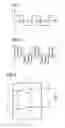
FIG. 1 shows an inventive distribution of the polarity of the capacitor voltage;
FIG. 2 shows an inventive distribution of the polarity of the capacitor voltage as a pulsating DC voltage; and
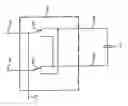
FIG. 3 shows a capacitor circuit arrangement according to the invention.
The following list of reference symbols can be used in conjunction with the figures:
| 1 | Capacitor |
| 2 | Changeover arrangement |
| 3 | First input |
| 4 | Second input |
| 5 | First switch |
| 6 | Second switch |
| 7 | Control line |
| 8 | First output |
| 9 | Second output |
| N | Event |
As illustrated in the drawings, the polarity at the capacitor 1 changes as a result of a regular event N, which can be selected depending on the application. The event N is formed by applying the operating voltage to the semiconductor component or by an internally generated clock.
In this exemplary embodiment, the capacitor comprises two TiN electrodes and an SiN dielectric, which is surrounded by the electrodes.
FIG. 3 illustrates a changeover arrangement 2 that is implemented using conventional components and is intended to reverse the polarity at the capacitor 1. The capacitor circuit arrangement includes a first input 3 and a second input 4 as well as a changeover arrangement 2 that contains a first switch 5 and a second switch 6. Both switches can be electronically controlled using a control line 7. The changeover arrangement 2 has a first output 8 and a second output 9 which equally constitute the inputs of the capacitor 1.
If a control signal that is triggered by an event N is applied to the control line 7, the switches 5 and 6 are operated and the connections between the first input 3 and the first output 8 and between the second input 4 and the second output 9 are mutually interchanged. Depending on the signal applied and on the basis of the event N, capacitor voltage profiles as illustrated in FIG. 1 or FIG. 2 thus result.
The effect achieved in this case is that it becomes possible to now operate a capacitor, which has previously been operated in a purely unipolar manner, in a bipolar manner using a change in polarity and thus to significantly extend the lifetime of the capacitor.
In order to make optimum use of the effect to extend the lifetime of the capacitor, the stress levels of both polarities should compensate for each other.
For applications in which the capacitor is operated using a DC voltage, it is, therefore, necessary for the cumulated time during which the capacitor is operated with the first polarity to be approximately equal to the cumulated time during which the capacitor is operated with the second polarity. This type of application is preferred for use of the invention.
For applications in which the capacitor is operated using a voltage that varies over time, the time integral from the product of time and a suitable function of the voltage must be approximately compensated for with both polarities.
In order to carry out the method according to the invention, the originally applied capacitor voltage may be both a constant DC voltage and/or a pulsating DC voltage. The method can thus be applied to all capacitors that are operated in a unipolar manner.
In order to achieve the desired effect, the first and second periods of time may be seconds to weeks.
In another variant of the method according to the invention, the changeover arrangement is driven using a control signal. This has the advantage of possible automation of the changes in polarity of the capacitor voltage. It is possible to use the application of the operating voltage to the semiconductor component as the control signal. It is also possible to use an internally generated clock as the control signal. The advantage of one of these two embodiments of the method is that the polarity of the capacitor voltage is changed over in a completely automatic manner.
The considerable extension of the lifetime of the capacitor, which is achieved by means of the invention, can be used to increase the reliability and lifetime of the capacitor and thus of the overall semiconductor component. On the other hand, it is possible to reduce the thickness of the dielectric, which is required for a desired lifetime, and thus to reduce the space required by the capacitor in the semiconductor component.
Claims
What is claimed is:1. A semiconductor device comprising:
a first capacitor node;
a second capacitor node;
a first capacitor electrode;
a second capacitor electrode;
a capacitor dielectric disposed between the first capacitor electrode and the second capacitor electrode;
a first switch coupled between the first capacitor electrode and the first and second capacitor nodes such that the first switch has a first position that couples the first capacitor electrode to the first capacitor node and a second position that couples the first capacitor electrode to the second capacitor node; and
a second switch coupled between the second capacitor electrode and the first and second capacitor nodes such that the second switch has a first position that couples the second capacitor electrode to the first capacitor node and a second position that couples the second capacitor electrode to the second capacitor node.
2. The device of claim 1, further comprising a single control line coupled to both the first switch and the second switch.
3. The device of claim 2, wherein the single control line carries a control periodic signal.
4. The device of claim 1, wherein the first capacitor node always carries a voltage that is greater than or equal to a voltage carried on the second capacitor node.
5. The device of claim 4, wherein the first capacitor carries a fixed voltage.
6. A semiconductor device comprising:
a first capacitor electrode;
a second capacitor electrode;
a dielectric between the first capacitor electrode and the second capacitor electrode;
a changeover arrangement having a first input and a second input and a first output and a second output, wherein, in order to connect the capacitor, the first input constitutes the terminal for the first capacitor electrode and the second input constitutes the terminal for the second capacitor electrode, and the first output is connected to the first capacitor electrode and the second output is connected to the second capacitor electrode, and in which case, in a first switch position in the changeover arrangement, the first input is connected to the first output and the second input is connected to the second output and, in a second switch position, the first input is connected to the second output and the second input is connected to the first output.
7. The device of claim 6, wherein the changeover arrangement has a control input that controls the switch position.
8. The device of claim 7, wherein the control input is coupled to a control signal generator.
9. A method for driving a capacitor in a semiconductor component, the method comprising:
(a) generating a first voltage between a first node and a second node;
(b) for a first period of time, applying the first voltage to a capacitor by coupling a first capacitor electrode to the first node and coupling a second capacitor electrode to the second node;
(c) for a second period of time after the first period of time, applying the first voltage to the capacitor by coupling the first capacitor electrode to the second node and coupling the second capacitor electrode to the first node; and
(d) repeating steps (b) and (c).
10. The method as claimed in claim 9, wherein repeating steps (b) and (c) comprises continuously repeating steps (b) and (c).
11. The method as claimed in claim 10, wherein the sum of the first periods of time and the sum of the second periods of time are approximately the same.
12. The method as claimed in claim 10, wherein the magnitude of time integrals of a voltage function of the first periods of time and the magnitude of time integrals of a voltage function of the second periods of time are approximately the same.
13. The method as claimed in claim 9, wherein generating a first voltage comprises generating a pulsating DC voltage.
14. The method as claimed in claim 9, wherein the first period of time and the second period of time are each less than ten seconds.
15. The method as claimed in claim 9, wherein the first period of time and the second period of time are each at least one week.
16. The method as claimed in claim 9, wherein a point of time between the first period of time and the second period of time is controlled by a control signal.
17. The method as claimed in claim 16, wherein the control signal is generated whenever an operating voltage is applied to the semiconductor component.
18. The method as claimed in claim 16, wherein the control signal is internally generated from an internal clock in the semiconductor component.
19. The method as claimed in claim 9, wherein generating a voltage comprises generating a voltage characterized in that a potential at the first node is always greater than or equal to a potential at the second node.
20. The method as claimed in claim 19, wherein generating a voltage comprises generating a DC voltage.
Images & Drawings included:
Sources:
- United States Patent and Trademark Office - verify current appl. status at the USPTO↗
Recent applications in this class:
- » 20250125631 2025-04-17
CIRCUIT ARRANGEMENT AND METHOD FOR DISCHARGING A BIAS TEE CAPACITOR AND QUANTUM SIGNAL GENERATOR WITH SAID CIRCUIT ARRANGEMENT - » 20240388104 2024-11-21
METHODS OF USE OF ULTRA HIGH CAPACITY PERFORMANCE BATTERY CELL - » 20240266841 2024-08-08
Fast Charging Method and System, Terminal, and Charger - » 20240243586 2024-07-18
Photovoltaic Module - » 20240178675 2024-05-30
HALF-BRIDGE CIRCUIT USING MONOLITHIC FLIP-CHIP GAN POWER DEVICES - » 20230396073 2023-12-07
SYSTEM AND METHOD FOR A PORTABLE ELECTRONIC DEVICE CASE ASSEMBLY - » 20230336002 2023-10-19
BIDIRECTIONAL POWER MANAGEMENT TECHNIQUES - » 20230283085 2023-09-07
Electronic device fast charging method, apparatus, and device - » 20230155392 2023-05-18
Fast charging method and system, terminal, and charger - » 20230111993 2023-04-13
Half-bridge circuit using separately packaged GaN power devices
Recent applications for this Assignee:
- » 20190222018 2019-07-18
Temperature sensing and fault detection for paralleled double-side cooled power modules - » 20190120879 2019-04-25
Readout circuit for resistive and capacitive sensors - » 20170125556 2017-05-04
Tunnel field effect transistors - » 20160072383 2016-03-10
System and method for a controlled feedback charge pump - » 20160064451 2016-03-03
Semiconductor component comprising magnetic field sensor - » 20150137309 2015-05-21
Methods of fabricating isolation regions of semiconductor devices and structures thereof - » 20120278520 2012-11-01
System and method of transmitting data between devices connected via a bus defining a time slot during transmission for responsive output information from bus devices - » 20120199909 2012-08-09
Semiconductor devices and methods of manufacture thereof - » 20120162924 2012-06-28
Integrated Semiconductor Outline Package - » 20120081105 2012-04-05
Signal generation for spectral measurements