Device and method for including passive components in a chip scale package
US20060263939A1
2006-11-23
11/460,859
2006-07-28
✅ Patent granted
US 7,449,364 B2
2008-11-11
-
-
Luan Thai
2027-01-22
Abstract:
The invention provides a method and device for building one or more passive components into a chip scale package. The method includes the steps of selecting a passive component having a terminal pitch that is a multiple of the package ball pitch of a chip scale package and mounting the selected passive component terminals to ball sites of the package. A preferred embodiment of the invention uses a single metal layer polyamide tape as the substrate of the package. Additional preferred embodiments of the invention are disclosed in which the terminal pitch multiple of the package ball pitch is one or two. Devices corresponding to the disclosed methods are also disclosed.
Assignee:
- TEXAS INSTRUMENTS INCORPORATED 18,931 🇺🇸 Dallas, TX, United States
Interested in similar patents?
Get notified when new applications in this technology area are published.
Classification:
H01L23/48 IPC
Details of semiconductor or other solid state devices Arrangements for conducting electric current to or from the solid state body in operation, e.g. leads, terminal arrangements ; Selection of materials therefor
H01L23/49816 » CPC main
Details of semiconductor or other solid state devices; Arrangements for conducting electric current to or from the solid state body in operation, e.g. leads, terminal arrangements ; Selection of materials therefor consisting of soldered constructions; Leads, on insulating substrates,; Additional leads joined to the metallisation on the insulating substrate, e.g. pins, bumps, wires, flat leads Spherical bumps on the substrate for external connection, e.g. ball grid arrays [BGA]
H05K1/113 » CPC further
Printed circuits; Details; Printed elements for providing electric connections to or between printed circuits; Pads for surface mounting, e.g. lay-out directly combined with via connections Via provided in pad; Pad over filled via
H05K1/113 » CPC further
Printed circuits; Details; Printed elements for providing electric connections to or between printed circuits; Pads for surface mounting, e.g. lay-out directly combined with via connections Via provided in pad; Pad over filled via
H05K1/0231 » CPC further
Printed circuits; Details; Electrical arrangements not otherwise provided for; Reduction of cross-talk, noise or electromagnetic interference using auxiliary mounted passive components or auxiliary substances Capacitors or dielectric substances
H05K1/0231 » CPC further
Printed circuits; Details; Electrical arrangements not otherwise provided for; Reduction of cross-talk, noise or electromagnetic interference using auxiliary mounted passive components or auxiliary substances Capacitors or dielectric substances
H05K3/3442 » CPC further
Apparatus or processes for manufacturing printed circuits; Assembling printed circuits with electric components, e.g. with resistor electrically connecting electric components or wires to printed circuits by soldering; Surface mounted components; Leadless components having edge contacts, e.g. leadless chip capacitors, chip carriers
H05K3/3452 » CPC further
Apparatus or processes for manufacturing printed circuits; Assembling printed circuits with electric components, e.g. with resistor electrically connecting electric components or wires to printed circuits by soldering Solder masks
H05K3/3452 » CPC further
Apparatus or processes for manufacturing printed circuits; Assembling printed circuits with electric components, e.g. with resistor electrically connecting electric components or wires to printed circuits by soldering Solder masks
H05K3/4038 » CPC further
Apparatus or processes for manufacturing printed circuits; Forming printed elements for providing electric connections to or between printed circuits Through-connections; Vertical interconnect access [VIA] connections
H05K3/4038 » CPC further
Apparatus or processes for manufacturing printed circuits; Forming printed elements for providing electric connections to or between printed circuits Through-connections; Vertical interconnect access [VIA] connections
H05K2201/0305 » CPC further
Indexing scheme relating to printed circuits covered by; Conductive materials; Properties and characteristics in general Solder used for other purposes than connections between PCB or components, e.g. for filling vias or for programmable patterns
H05K2201/0305 » CPC further
Indexing scheme relating to printed circuits covered by; Conductive materials; Properties and characteristics in general Solder used for other purposes than connections between PCB or components, e.g. for filling vias or for programmable patterns
H05K2201/0394 » CPC further
Indexing scheme relating to printed circuits covered by; Conductive materials; Structure of the conductor; Other aspects of conductors Conductor crossing over a hole in the substrate or a gap between two separate substrate parts
H05K2201/0394 » CPC further
Indexing scheme relating to printed circuits covered by; Conductive materials; Structure of the conductor; Other aspects of conductors Conductor crossing over a hole in the substrate or a gap between two separate substrate parts
H05K2201/09772 » CPC further
Indexing scheme relating to printed circuits covered by; Shape and layout; Shape and layout details of conductors covering at least two types of conductors provided for in - Conductors directly under a component but not electrically connected to the component
H05K2201/09772 » CPC further
Indexing scheme relating to printed circuits covered by; Shape and layout; Shape and layout details of conductors covering at least two types of conductors provided for in - Conductors directly under a component but not electrically connected to the component
H05K2201/10636 » CPC further
Indexing scheme relating to printed circuits covered by; Details of components or other objects attached to or integrated in a printed circuit board; Details of electrical connections of non-printed components, e.g. special leads; Components characterised by their electrical contacts Leadless chip, e.g. chip capacitor or resistor
Y02P70/50 » CPC further
Climate change mitigation technologies in the production process for final industrial or consumer products Manufacturing or production processes characterised by the final manufactured product
Y02P70/50 » CPC further
Climate change mitigation technologies in the production process for final industrial or consumer products Manufacturing or production processes characterised by the final manufactured product
H01L2924/0002 » CPC further
Indexing scheme for arrangements or methods for connecting or disconnecting semiconductor or solid-state bodies as covered by; Technical content checked by a classifier Not covered by any one of groups , and
H01L2924/00 » CPC further
Indexing scheme for arrangements or methods for connecting or disconnecting semiconductor or solid-state bodies as covered by
H01L21/00 IPC
Processes or apparatus adapted for the manufacture or treatment of semiconductor or solid state devices or of parts thereof
H01L21/50 IPC
Processes or apparatus adapted for the manufacture or treatment of semiconductor or solid state devices or of parts thereof; Manufacture or treatment of semiconductor devices or of parts thereof the devices having at least one potential-jump barrier or surface barrier, e.g. PN junction, depletion layer or carrier concentration layer Assembly of semiconductor devices using processes or apparatus not provided for in a single one of the subgroups - , e.g. sealing of a cap to a base of a container
H01L21/48 IPC
Processes or apparatus adapted for the manufacture or treatment of semiconductor or solid state devices or of parts thereof; Manufacture or treatment of semiconductor devices or of parts thereof the devices having at least one potential-jump barrier or surface barrier, e.g. PN junction, depletion layer or carrier concentration layer Manufacture or treatment of parts, e.g. containers, prior to assembly of the devices, using processes not provided for in a single one of the subgroups -
H01L21/44 IPC
Processes or apparatus adapted for the manufacture or treatment of semiconductor or solid state devices or of parts thereof; Manufacture or treatment of semiconductor devices or of parts thereof the devices having at least one potential-jump barrier or surface barrier, e.g. PN junction, depletion layer or carrier concentration layer the devices having semiconductor bodies not provided for in groups, , , and with or without impurities, e.g. doping materials Manufacture of electrodes on semiconductor bodies using processes or apparatus not provided for in groups -
H01L23/52 IPC
Details of semiconductor or other solid state devices Arrangements for conducting electric current within the device in operation from one component to another, i.e. interconnections, e.g. wires, lead frames
H01L23/40 IPC
Details of semiconductor or other solid state devices; Arrangements for cooling, heating, ventilating or temperature compensation ; Temperature sensing arrangements Mountings or securing means for detachable cooling or heating arrangements ; fixed by friction, plugs or springs
Description
PRIORITY DATEThis is a divisional application of co-pending application Ser. No. 10/103,386 filed Mar. 21, 2002, the contents of which are herein incorporated by reference in its entirety, which claims the benefit of U.S. Provisional Application No. 60/344,200, filed Dec. 28, 2001.
TECHNICAL FIELDThe invention relates to devices and methods for packaging integrated circuit (IC) devices. More particularly, the invention relates to the packaging of ICs with accompanying discrete passive components on the same chip package by forming direct connections between substrate solder balls and IC and discrete component terminals or pads.
BACKGROUND OF THE INVENTIONIn use, integrated circuits (ICs) generally require electrical connections to a substrate to form a package providing electrical connections to additional electronic devices. In general, in a ball grid array (BGA), an approximately square package substrate is provided with solder balls for electrical connection to IC terminals or bonding pads. The package substrate may be composed of multiple layers of semiconductor, mask, and conductive materials depending upon the complexity of the electrical connections to be made. In practice, the more layers, the higher the manufacturing effort and expense.
IC dice may be packaged alone, but frequently an IC die is included on a package substrate along with one or more discrete passive components such as resistors, capacitors, and so forth. Including discrete passive components in an IC package typically adds significant development and manufacturing costs and design complexity to the packaging endeavor. This complexity is engendered by the need for engineering changes to the package to accommodate the interconnection of the components selected for a particular application. Generally, expenses and complexity are also increased by the necessity of using multiple layer substrates in order to make electrical connections among the various discrete component terminals, IC terminals, and ball sites of the substrate.
Methods and devices providing the capability of including discrete passive components in an IC chip scale package with reduced cost and a reduced need for engineering changes to the package would be desirable in the arts.
SUMMARY OF THE INVENTIONIn general, devices and methods providing for the inclusion of electrically connected discrete components and ICs in a single chip package with reduced complexity and expense are disclosed.
According to one aspect of the invention, a method of building one or more passive components into an existing chip scale package includes the steps of selecting a passive component having a terminal pitch that is a multiple of the package ball pitch of a chip scale package and mounting the passive component terminals or pads directly to ball sites of the package.
According to another aspect of the invention, a single metal layer polyamide tape is selected for use as the substrate of the package.
According to still another aspect of the invention, a chip scale package device has at least one IC and at least one discrete passive component connected to a package having a preselected ball pitch. The IC terminals or pads, as well as those of the discrete passive component, are coupled directly to ball sites of the package. In order to facilitate direct coupling, the discrete passive component has a terminal pitch that is a multiple of the package ball pitch.
Technical advantages are provided by the invention, including but not limited to reduced design complexity when engineering a package for selected ICs and discrete passive components. Reduced expense through the use of single metal layer substrate and the avoidance of multiple metal layer substrate. Reduced design and test times due to the ready connectablitity of components facilitated by the invention. These and many other advantages related to the improvements of the invention will become apparent to persons skilled in the relevant arts through careful reading of the disclosure and claims presented herein.
BRIEF DESCRIPTION OF THE DRAWINGSFor a better understanding of the invention including its features, advantages and specific embodiments, reference is made to the following detailed description along with accompanying drawings in which:
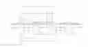
FIG. 1 depicts a top view of a package showing an example of the invention; and
FIG. 2 shows a cross-sectional view of a portion of FIG. 1 taken along line 2-2 of FIG. 1.
References in the detailed description correspond to like references in the figures unless otherwise noted. Like numerals refer to like parts throughout the various figures. The descriptive and directional terms used in the written description such as top, bottom, left, right, etc., refer to the drawings themselves as laid out on the paper and not to physical limitations of the invention unless specifically noted. The drawings are not to scale and some features of embodiments shown and discussed are simplified or exaggerated for illustrating the principles of the invention.
DETAILED DESCRIPTION OF PREFERRED EMBODIMENTSWhile the making and using of various embodiments of the present invention are discussed in detail below, it should be appreciated that the present invention provides many applicable inventive concepts which can be embodied in a wide variety of specific contexts. It should be understood that the invention may be practiced with dice and discrete devices of various types and materials without altering the principles of the invention.
A preferred embodiment of the invention is shown in the example of FIG. 1. A package 10 is based on a substrate 12, preferably a single metal layer tape substrate although double layer or other multi-layer substrates may also be used. The substrate 12 contains ball sites 14 arranged in a grid pattern and having standardized spacing. For example spacing, commonly referred to as “ball pitch”, of 0.50 millimeters, or 0.80 millimeters is known in the arts. Of course, many alternative pitches are possible. A semiconductor die, typically an IC 16, is mounted on a substrate 12 by connecting die terminals or pads (not shown in FIG. 1) to ball sites 14. Discrete passive components 18, such as resistors, capacitors, etc., are included on the substrate 12 as well. In the preferred embodiments of the invention, the discrete component 18 terminals 20 are connected directly to ball sites 14 of the substrate 12.
Thus the package 10 is completed without the need for additional electrical connections or leads on the substrate 12, avoiding the need in many cases for multilayer substrates. This direct package connection is achieved by the selection of a ball pitch for the package chosen to match the terminal pitch of the discrete component as further described with reference to FIG. 2 below.
FIG. 2 is a cross-section view taken along line 2-2 of FIG. 1. The single metal layer tape substrate 12 is shown with a discrete component 18 mounted thereon. The ball sites 14 are evenly spaced having a predetermined ball pitch B. The discrete component 18 has a predetermined terminal pitch indicated by T. According to the preferred embodiment of the invention, the substrate 12 ball pitch B is fabricated to match the terminal pitch T by some whole number multiple. For example, as shown in FIG. 2, the terminal pitch T is equal to two times the ball pitch B or, T=2×B. Typically, the discrete component 18 is joined to the substrate 12 by means of a conductive adhesive 28 to the via cap 24 of the ball site 14 at preselected locations where the solder mask 26 of the substrate 12 has been removed.
In the preferred embodiment of the invention represented in FIG. 2, the discrete component 18 is a “0402” component having a terminal pitch T of 1.0 millimeters and the ball pitch B of the substrate 12 has been chosen as 0.50 millimeters. This way, there is a direct correspondence between component terminals 20 and selected ball sites 14, facilitating the direct electrical connection of the discrete component 18 to the substrate 12 with minimal time and expense, advantageously avoiding the time and expense otherwise associated with the design and manufacture of horizontal and multi-layer connections. Of course, the values shown and described with reference to FIG. 2 are merely examples and are not intended to limit the practice of the invention to any particular numerical values. To cite but a few additional examples, “0603” discrete passive components may also be used, as may a substrate having a ball pitch of 1.0 millimeter.
The embodiments shown and described above are only exemplary. Even though numerous characteristics and advantages of the present invention have been set forth in the foregoing description together with details of the method and device of the invention, the disclosure is illustrative only and changes may be made within the principles of the invention to the full extent indicated by the broad general meaning of the terms used in the attached claims.
Claims
I claim:1. A method of building one or more passive components into an existing chip scale package comprising the steps of:
selecting a passive component having a terminal pitch that is a multiple of the package ball pitch of a chip scale package; and
mounting the selected passive component terminals to ball sites of the package.
2. The method of claim 1 further comprising the step of selecting a passive component wherein the terminal pitch multiple of the package ball pitch is one.
3. The method of claim 1 further comprising the step of selecting a passive component wherein the terminal pitch multiple of the package ball pitch is two.
4. The method of claim 1 further comprising the step of selecting a package having a ball pitch of 0.50 millimeters.
5. The method of claim 1 further comprising the step of selecting a package having a ball pitch of 1.0 millimeters.
6. The method of claim 1 further comprising the step of selecting a 0402 passive component.
7. The method of claim 1 further comprising the step of selecting a 0603 passive component.
8. The method of claim 1 further comprising the step of using a single conductive layer tape as the substrate of the package.
9. The method of claim 1 further comprising the step of using a single metal layer polyimide tape as the substrate of the package.
Images & Drawings included:

Sources:
- United States Patent and Trademark Office - verify current appl. status at the USPTO↗
Similar patent applications:
Recent applications in this class:
- » 20250273550 2025-08-28
SEMICONDUCTOR STRUCTURE AND MANUFACTURING METHOD THEREOF - » 20250273549 2025-08-28
MULTI-CHIP PACKAGE, METHOD FOR REDUCING PEAK CURRENT AND SEMICONDUCTOR DEVICE - » 20250266338 2025-08-21
SYSTEMS FOR SEMICONDUCTOR PACKAGE MOUNTING WITH IMPROVED CO-PLANARITY - » 20250266337 2025-08-21
CIRCUIT MODULE AND MOUNTING METHOD FOR CIRCUIT MODULE - » 20250266336 2025-08-21
SEMICONDUCTOR PACKAGE AND METHOD OF MANUFACTURING AND TESTING THE SAME - » 20250259919 2025-08-14
PACKAGE COMPRISING A SUBSTRATE AND A PASSIVE DEVICE - » 20250253221 2025-08-07
SEMICONDUCTOR PACKAGE AND METHOD OF FABRICATING THE SAME - » 20250233058 2025-07-17
SEMICONDUCTOR PACKAGE STRUCTURE AND METHOD OF FABRICATING THE SAME - » 20250210483 2025-06-26
SUBSTRATE, PACKAGING STRUCTURE, AND ELECTRONIC DEVICE - » 20250210482 2025-06-26
STACKED PACKAGE DEVICE WITH INTERCONNECTED CONDUCTIVE BUMPS
Recent applications for this Assignee:
- » 20250291595 2025-09-18
CIRCUIT, SYSTEM, AND METHOD FOR MATRIX DECIMATION - » 20250286550 2025-09-11
TRANSISTOR SHUTDOWN CIRCUT - » 20250279725 2025-09-04
CONDUCTION MODE CONTROL - » 20250274138 2025-08-28
SWITCH REGULATOR - » 20250267687 2025-08-21
ENHANCED BROADCAST TRANSMISSION IN UNSLOTTED CHANNEL HOPPING MEDIUM ACCESS CONTROL - » 20250266825 2025-08-21
BOOTSTRAP CIRCUIT - » 20250247097 2025-07-31
LEVEL SHIFTER CIRCUIT - » 20250247082 2025-07-31
LOW AREA AND POWER MULTI-BIT FLIP-FLOP - » 20250246995 2025-07-31
SWITCHING CONVERTER DEADTIME CONTROL - » 20250246345 2025-07-31
TRIMMING RESISTOR USING MODULATED SIGNAL