Photoresist coating composition and method for forming fine contact of semiconductor device
US20060269676A1
2006-11-30
11/296,826
2005-12-07
Abstract:
A coating composition containing a coating base resin and a C4-C10 alcohol as a main solvent, and a method for forming a fine contact of a semiconductor device including the steps of preparing the coating composition, forming a photoresist film on a semiconductor substrate having an underlying layer, performing exposure with a contact mask and developing processes to form a photoresist pattern for contact on the photoresist film, and coating the coating composition on the photoresist pattern to form a coating film.
Assignee:
- HYNIX SEMICONDUCTOR INC. 2,115 🇰🇷 Gyeonggi-do, South Korea
Interested in similar patents?
Get notified when new applications in this technology area are published.
Classification:
C09D133/08 » CPC main
Coating compositions based on homopolymers or copolymers of compounds having one or more unsaturated aliphatic radicals, each having only one carbon-to-carbon double bond, and at least one being terminated by only one carboxyl radical, or of salts, anhydrides, esters, amides, imides, or nitriles thereof; Coating compositions based on derivatives of such polymers; Homopolymers or copolymers of esters of esters containing only carbon, hydrogen and oxygen, the oxygen atom being present only as part of the carboxyl radical Homopolymers or copolymers of acrylic acid esters
G03F7/40 » CPC further
Photomechanical, e.g. photolithographic, production of textured or patterned surfaces, e.g. printing surfaces; Materials therefor, e.g. comprising photoresists; Apparatus specially adapted therefor; Processing photosensitive materials; Apparatus therefor Treatment after imagewise removal, e.g. baking
B05D5/00 IPC
Processes for applying liquids or other fluent materials to surfaces to obtain special surface effects, finishes or structures
B05D1/36 IPC
Processes for applying liquids or other fluent materials Successively applying liquids or other fluent materials, e.g. without intermediate treatment
Description
BACKGROUND OF THE DISCLOSURE1. Field of the Disclosure
The disclosure relates to a coating composition and a method for forming a fine contact of a semiconductor device using the same.
2. Description of the Related Technology
In order to overcome the resolution limit of exposures in forming a fine contact of a semiconductor device, a phase shift mask is typically used or a contact is heated at above the glass transition temperature of the photoresist to cause flow (known as a resist flow process, as described in U.S. Pat. No. 6,824,951, the disclosure of which is incorporated herein by reference). Otherwise, a RELACS (Resolution Enhancement Lithography Assisted by Chemical Shrink process, as described in “Resists Join the Sub-λ Revolution”, Semiconductor International, 1999. 9., Laura J. Peters ed., the disclosure of which is incorporated herein by reference,) process is performed to reduce the size of the contact, thereby obtaining a fine contact suitable for a high degree of integration of semiconductor devices.
However, when the phase shift mask is used, a side-lobe is generated or the resolution is degraded during the process for forming a pattern.
In the resist flow process, even when the same thermal energy is transmitted to the entire surface of the photoresist at over the glass transition temperature, the flowing amount of the photoresist is larger in the lower portion than in the upper or middle portion so as to cause an over-flow, with the space between the upper portion of the patterns is wider than the space between the lower portion of the patterns.
In the RELACS process, materials are expensive, and water-soluble polymers are not completely removed but remain on the pattern to affect subsequent etching processes. As a result, it is possible to generate defects in manufactured devices, thereby decreasing yield and reliability of devices.
Moreover, when a coating process is performed on the contact, the size of the formed contact can be smaller than the original one of the contact. However, since water is used as a solvent, coating properties may be degraded.
Although an organic solvent can be used to improve the coating properties, the organic solvent dissolves a lower photoresist layer. In order to prevent the lower photoresist layer from being dissolved by the organic solvent, the coating composition should be cross-linked after the contact is formed. For this cross-linking, an additional process such as electronic beam curing, thermal curing, or ultraviolet curing is required.
SUMMARY OF THE DISCLOSUREA coating composition contains a coating base resin and a C4-C10 alcohol as a main solvent, and a method for forming a fine contact sufficient for high integration of a semiconductor device including performing a coating process on a contact using the coating composition.
BRIEF DESCRIPTION OF THE DRAWINGSFor a more complete understanding of the invention, reference should be made to the following detailed description and accompanying drawings wherein:
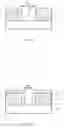
FIGS. 1a and 1b are cross-sectional diagram illustrating a method according to the disclosure for forming a fine contact of a semiconductor device;
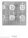
FIG. 2 is a SEM photograph illustrating a photoresist pattern for contact obtained from a Comparative Example;
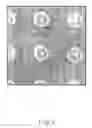
FIG. 3 is a SEM photograph illustrating a photoresist pattern for contact obtained from Example 4; and
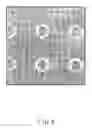
FIG. 4 is a SEM photograph illustrating a photoresist pattern for contact obtained from Example 5.
DETAILED DESCRIPTION OF PREFERRED EMBODIMENTSThe disclosed coating composition contains a coating base resin and C4-C10 alcohol as a main solvent.
The C4-C10 alcohol is preferably a compound selected from the group consisting of cyclopentanol, cycloheptanol, butanol, pentanol, hexanol, octanol, nonanol, decanol, and mixtures thereof. The alcohol solvent dissolves the lower photoresist layer when the carbon number is less than four, and the volatility of the solvent is so small to be used as a coating solvent when the number of carbon is more than ten.
The coating composition includes a coating base resin, and the coating base resin is preferably, but not necessarily, an acrylic resin. Herein the term “acrylic resin” means the resin produced essentially by polymerization of acrylic acid, methacrylic acid and derivatives thereof. A preferred example of acrylic resin is poly(t-butylacrylate/methacrylic acid/methacrylate).
The disclosure also provides a method for forming a fine contact of a semiconductor device.
The method includes the steps of:
-
- (a) preparing a coating composition according to the disclosure;
- (b) forming a photoresist film on a semiconductor substrate having an underlying layer;
- (c) performing exposure with a contact mask and a developing process to form a photoresist pattern for contact on the photoresist film; and
- (d) coating the coating composition on the photoresist pattern to form a coating film.
Preferably, the method further includes the step of performing a resist flow process or the step of performing a RELACS (Resolution Enhancement Lithography Assisted by Chemical Shrink) process onto the photoresist pattern after step (b) and before step (c) in order to form a fine contact having a smaller contact region.
The disclosure will be described in detail with FIGS. 1a and 1b.
Referring to FIG. 1a, a photoresist composition is coated on a semiconductor substrate 11 having an underlying layer to form a photoresist film.
Next, a photoresist film 13 containing a contact region 15 is formed by an exposure and developing process with a contact mask (not shown).
The contact region 15 is formed to have a diameter (a).
Referring to FIG. 1b, a coating composition is coated on the entire surface including the contact region 15 to form a coating film 17 having a thickness ranging from 20 nm to 100 nm.
The coating composition obtained by dissolving acrylic resin as a base resin in C4-C10 alcohol as a main solvent is applied by simple spin-coating to form a coating film 17 by volatilization of the alcohol. The additional process such as the curing process is not required since the C4-C10 alcohol does not dissolve the lower photoresist layer.
As a result, the coating film 17 reduces a diameter of the contact region 15 into the size (b).
The diameter of the contact region 15 can be adjusted depending on the thickness of the coating film 17.
As described above, the size of the contact region 15 is changed by regulation of the thickness of the disclosed coating film 17, and the thickness of the coating film 17 can be regulated as intended to improve reproducibility of the process and minimize characteristic change of devices, thereby facilitating high-integration of semiconductor devices.
Before the coating film 17 is formed, the photoresist pattern 13 can be heated at over a glass transition temperature of photoresist to cause flow or a RELACS process can be performed, forming the diameter of the contact region 15 to be smaller than (a) in advance, and then the coating film 17 is formed. As a result, the diameter of the contact region can be regulated to be even smaller.
EXAMPLESThe disclosure will be described in details by referring to examples below, which are given to illustrate not to limit the disclosed coating compounds and method.
Example 1 Preparation of a Coating Base ResinTo acetone (50 g) were dissolved t-butylacrylate (5.0 g), methacrylic acid (2.0 g), methacrylate (3.0 g) and AIBN (2,2′-azobisisobutyronitrile) (0.02 g) as a polymerization initiator, and then the resulting mixture was polymerized at about 67° C. for about 6 hours. After polymerization is completed, the resulting mixture was filtered and vacuum dried to obtain poly(t-butylacrylate/methacrylic acid/methacrylate) (yield: 88%).
Example 2 Preparation of a Coating Composition (1)The poly(t-butylacrylate/methacrylic acid/methacrylate) (1 g) obtained from Example 1 was dissolved in cycloheptanol (80 g) to obtain a coating composition.
Example 3 Preparation of a Coating Composition (2)The poly(t-butylacrylate/methacrylic acid/methacrylate) (1 g) obtained from Example 1 was dissolved in cyclopentanol (70 g) to obtain a disclosed coating composition.
Comparative Example Formation of a Photoresist Pattern for Contact (1)An ArF photoresist composition 7039R (produced by TOK Co.) was coated on a silicon wafer, and soft-baked at about 120° C. for about 90 seconds. After soft-baking, the photoresist film was exposed to light using an ArF laser Scanner XT:1400E (ASML Inc.), and post-baked at about 120° C. for about 90 seconds. After post-baking, it was developed in 2.38 wt % tetramethylammonium hydroxide (TMAH) aqueous solution for about 40 seconds, to obtain a 134 nm photoresist pattern for contact (see FIG. 2).
Example 4 Formation of a Photoresist Pattern for Contact (2)The coating composition obtained from Example 2 was spin-coated on the 134 nm photoresist pattern for contact shown in FIG. 2 by the same procedure of Comparative Example to obtain a 105 nm photoresist pattern (see FIG. 3).
That is, by forming the coating film with cycloheptanol as the alcohol solvent having the number of carbon of over 4, the obtained photoresist pattern for contact was smaller by 29 nm than the photoresist pattern for contact obtained from Comparative Example where the coating film was not formed.
Example 5 Formation of a Photoresist Pattern for Contact (3)The coating composition obtained from Example 3 was spin-coated on the 134 nm photoresist pattern for contact shown in FIG. 2 by the same procedure of Comparative Example to obtain a 98 nm photoresist pattern (see FIG. 4).
That is, by forming the coating film with cyclopentanol as the alcohol solvent having the number of carbon of over 4, the obtained photoresist pattern for contact was smaller by 36 nm than the photoresist pattern for contact obtained from Comparative Example where the coating film was not formed.
As described above, in order to obtain a fine contact, a contact is first formed, and a coating composition using a C4-C10 alcohol as a main solvent for coating composition is coated thereon to form a coating film. As a result, the photoresist pattern for contact having a smaller contact region can be obtained rather than when the coating film is not formed.
Claims
What is claimed is:1. A coating composition comprising a coating base resin and a C4-C10 alcohol as a main solvent.
2. A composition of claim 1, wherein the C4-C10 alcohol is present in an amount ranging from about 400 g to 4000 g based on 100 g of the coating base resin.
3. A composition of claim 1, wherein the coating base resin is an acrylic resin.
4. A composition of claim 3, wherein the acrylic resin is poly(t-butylacrylate/methacrylic acid/methacrylate).
5. A composition of to claim 1, wherein the C4-C10 alcohol is a compound selected from the group consisting of cyclopentanol, cycloheptanol, butanol, pentanol, hexanol, octanol, nonanol, decanol, and mixtures thereof.
6. A composition according to claim 1, wherein the composition consists essentially of a coating base resin and a C4-C10 alcohol as a main solvent
7. A method for forming a fine contact of a semiconductor device, comprising the steps of:
(a) providing a coating composition according to claim 1;
(b) forming a photoresist film on a semiconductor substrate having an underlying layer;
(c) performing exposure with a contact mask and a developing process to form a photoresist pattern for contact on the photoresist film; and
(d) coating the coating composition on the photoresist pattern to form a coating film.
8. The method of claim 7, further comprising the step of performing a resist flow process onto the photoresist pattern after step (b) and before step (c).
9. The method of claim 7, further comprising the step of performing a RELACS (Resolution Enhancement Lithography Assisted by Chemical Shrink) process onto the photoresist pattern after step (b) and before step (c).
10. The method of claim 7, comprising forming the coating film to a thickness in the range of 20 nm to 100 nm.
Images & Drawings included:
Sources:
- United States Patent and Trademark Office - verify current appl. status at the USPTO↗
Similar patent applications:
Recent applications in this class:
- » 20250145849 2025-05-08
TOP COAT COMPOSITION - » 20250109314 2025-04-03
MOISTURE ABSORPTION FILM LAYERED PRODUCT AND MANUFACTURING METHOD THEREFOR - » 20250101250 2025-03-27
NON-FLUORINATED SURFACTANTS FOR FLOOR CARE COATINGS - » 20250092281 2025-03-20
AQUEOUS COATING COMPOSITION AND METHOD FOR PRODUCING AQUEOUS COATING COMPOSITION - » 20250011614 2025-01-09
AQUEOUS DISPERSION, AND FILM AND LAMINATED BODY USING THE SAME - » 20240425716 2024-12-26
WATER-RESISTANT ACRYLIC COATINGS - » 20240384126 2024-11-21
Finish Coat Composition, Composite Material, Middle Frame of Electronic Device, Housing of Electronic Device, and Electronic Device - » 20240376338 2024-11-14
BIOBASED LATEX HAVING INCREASED C14 CONTENT, METHODS OF MAKING AND METHODS OF USING - » 20240368424 2024-11-07
PCM COATING ON THE FILLER MATERIAL - » 20240343933 2024-10-17
PRINTING SHEET AND METHOD FOR PRODUCING PRINTING SHEET
Recent applications for this Assignee:
- » 20130182518 2013-07-18
Memory cell of semiconductor memory device and method for driving the same - » 20130182504 2013-07-18
Page buffer circuit and nonvolatile memory device having the same - » 20130166940 2013-06-27
Semiconductor device for generating initialization of information in response to a first clock and outputting the initialization information in response to a second clock - » 20130166823 2013-06-27
Non-volatile memory device for storing write data having different logic levels - » 20130163366 2013-06-27
Semiconductor memory device and operation method thereof - » 20130163352 2013-06-27
Semiconductor memory device - » 20130162321 2013-06-27
Semiconductor device including driving circuit - » 20130162274 2013-06-27
Semiconductor integrated circuit and test control method thereof - » 20130161710 2013-06-27
Semiconductor device having buried bit line and method for fabricating the same - » 20130157461 2013-06-20
Method for fabricating semiconductor memory device