Forming a conductive pattern on a substrate
US20060273069A1
2006-12-07
11/146,498
2005-06-06
✅ Patent granted
US 7,271,099 B2
2007-09-18
-
-
Nadine Norton | Maki Angadi
2025-08-30
Abstract:
A method of forming a conductive pattern on a substrate. The method comprising providing a substrate carrying a conductive layer; forming a first portion of the conductive pattern by exposing the conductive layer to a laser and controlling the laser to remove conductive material around the edge(s) of desired conductive region(s) of the first portion; and laying down an etch resistant material on the conductive layer, the etch resistant material defining a second portion of the conductive pattern, removing conductive material from those areas of the second portion not covered by the etch resistant material, and then removing the etch resistant material.
Inventors:
- Martin Philip Gouch 9 🇬🇧 Herts, United Kingdom
- Nigel Ingram Bromley 2 🇬🇧 Milton Keynes, United Kingdom
- Christoph Bittner 3 🇬🇧 Herts, United Kingdom
Assignee:
- FFEI LIMITED 15 🇬🇧 Hertfordshire, United Kingdom
- FUJIFILM ELECTRONIC IMAGING LTD. 9 🇬🇧 Hertfordshire, United Kingdom
Interested in similar patents?
Get notified when new applications in this technology area are published.
Classification:
H05K3/027 » CPC main
Apparatus or processes for manufacturing printed circuits in which the conductive material is applied to the surface of the insulating support and is thereafter removed from such areas of the surface which are not intended for current conducting or shielding the conductive material being removed by irradiation, e.g. by photons, alpha or beta particles
H05K3/061 » CPC further
Apparatus or processes for manufacturing printed circuits in which the conductive material is applied to the surface of the insulating support and is thereafter removed from such areas of the surface which are not intended for current conducting or shielding the conductive material being removed chemically or electrolytically, e.g. by photo-etch process Etching masks
H05K2201/09363 » CPC further
Indexing scheme relating to printed circuits covered by; Shape and layout; Shape and layout details of conductors; Conductive planes wherein only contours around conductors are removed for insulation
H05K2201/09363 » CPC further
Indexing scheme relating to printed circuits covered by; Shape and layout; Shape and layout details of conductors; Conductive planes wherein only contours around conductors are removed for insulation
H05K2203/013 » CPC further
Indexing scheme relating to apparatus or processes for manufacturing printed circuits covered by; Tools for processing; Objects used during processing for patterning or coating Inkjet printing, e.g. for printing insulating material or resist
H05K2203/013 » CPC further
Indexing scheme relating to apparatus or processes for manufacturing printed circuits covered by; Tools for processing; Objects used during processing for patterning or coating Inkjet printing, e.g. for printing insulating material or resist
H05K2203/1476 » CPC further
Indexing scheme relating to apparatus or processes for manufacturing printed circuits covered by; Related to the order of processing steps Same or similar kind of process performed in phases, e.g. coarse patterning followed by fine patterning
H05K2203/1476 » CPC further
Indexing scheme relating to apparatus or processes for manufacturing printed circuits covered by; Related to the order of processing steps Same or similar kind of process performed in phases, e.g. coarse patterning followed by fine patterning
Y10T428/24917 » CPC further
Stock material or miscellaneous articles; Structurally defined web or sheet [e.g., overall dimension, etc.]; Discontinuous or differential coating, impregnation or bond [e.g., artwork, printing, retouched photograph, etc.] including metal layer
Y10T428/24926 » CPC further
Stock material or miscellaneous articles; Structurally defined web or sheet [e.g., overall dimension, etc.]; Discontinuous or differential coating, impregnation or bond [e.g., artwork, printing, retouched photograph, etc.] including ceramic, glass, porcelain or quartz layer
C23F1/00 IPC
Etching metallic material by chemical means
B44C1/22 IPC
Processes, not specifically provided for elsewhere, for producing decorative surface effects Removing surface-material, e.g. by engraving, by etching
C03C15/00 IPC
Surface treatment of glass; Surface treatment of fibres or filaments from glass, minerals or slags
C03C15/00 IPC
Surface treatment of glass, not in the form of fibres or filaments, by etching
H01L21/76 IPC
Processes or apparatus adapted for the manufacture or treatment of semiconductor or solid state devices or of parts thereof; Manufacture or treatment of devices consisting of a plurality of solid state components formed in or on a common substrate or of parts thereof; Manufacture of integrated circuit devices or of parts thereof; Manufacture of specific parts of devices defined in group Making of isolation regions between components
Description
The invention relates to a method of forming a conductive pattern on a substrate, for example so as to form an electronic circuit.
In one approach to forming very high resolution electrical circuits, for example that used by LPKF Laser and Electronics AG of Germany, a laser is used to cut a narrow line through a layer of a conductive material on an insulating substrate. Complete loops of such cuts are used to isolate areas of conductor which then become the conductive traces of the circuit. This process is useful for forming prototype circuit boards but is slow and the resulting circuit has large areas of unwanted conductor remaining. These are normally left in place since it would take a very long time to use the laser to remove them.
An alternative approach which can be used for low resolution circuits is to define the required circuit as a rasterised image which is then printed, typically using an ink jet printer, over the whole area of the conductive layer using an ink capable of resisting a chemical etch. The required circuit pattern is then produced by etching the conductive layer where it is not covered with the ink, and then removing the ink using another chemical such as a solvent. This process is suitable for producing small volume or prototype products as it is reasonably fast and economical with materials but is not capable of high resolution. This is because of the rasterisation process and the unpredictable behaviour of the printing heads and of the ink on the surface.
In accordance with the present invention, a method of forming a conductive pattern on a substrate comprises:
-
- a) providing a substrate carrying a conductive layer;
- b) forming a first portion of the conductive pattern by exposing the conductive layer to a laser and controlling the laser to remove conductive material around the edge(s) of desired conductive region(s) of the first portion; and,
- c) laying down an etch resistant material on the conductive layer, the etch resistant material defining a second portion of the conductive pattern, removing conductive material from those areas of the second portion not covered by the etch resistant material, and then removing the etch resistant material.
We have realized that typical circuits have some areas requiring high resolution, for example tracks around high density Ball Grid Array (BGA) chips, and other, normally larger areas, where a lower resolution is adequate. It is then possible to optimize the use of the two techniques so that the laser process is only used in those areas requiring high resolution and the etch process is used in the remaining, low resolution areas.
In some cases, the etch resistant material could be confined to the second portion but this has the disadvantage that it is necessary to prevent the removal chemical from reaching the first portion. Preferably, therefore, the etch resistant material at least overlaps the conductive regions of the first portion and preferably is laid down as a solid block over the whole of the first portion.
Typically, the etch resistant material will be printed, for example using an ink jet printer or other conventional printer.
An example of a method according to the invention will now be described with reference to the accompanying drawings, in which:—
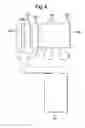
FIGS. 1A and 1B are a plan and schematic cross-section of a substrate carrying a conductive layer; and,
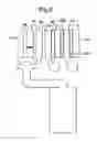
FIGS. 2 to 5 illustrate plan views of the conductive layer at successive stages during the process.
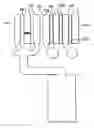
FIGS. 1A and 1B illustrate an insulating substrate 1 on which is provided a continuous, conductive, e.g. copper, surface layer 2.
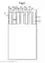
In the first stage of the process, a first portion 3 of the copper layer 2 is exposed to a laser beam (not shown). A suitable beam could be generated from a neodymium YAG or frequency-doubled YAG laser. The laser beam is controlled to define the edges of desired conductive regions 4A-4G by removing or ablating thin lines of the conducting material as shown at 5A-5G. Portions of the substrate 1 can be seen through the regions 5A-5G. A resolution better than 100 μm is achieved, even to 25 μm.
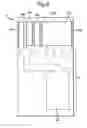
In the next step (FIG. 3), an etch resist ink 20, such as Jetrack Etch Resist 001 from Avecia Electronic Materials, is applied using an ink jet printer (not shown) onto the surface of the copper layer 2. In the portion 6, this etch resist ink defines the desired circuit pattern at a relatively low resolution, e.g. 100 μm or more. In the portion 3, the etch resist ink is laid down in regions 10A-10C on previously defined conductive regions 4A-4C so as slightly to overlap the corresponding etch lines 5A-5C. In addition, a solid block of the etch resist ink 10D is laid down over all the regions 4D-4G. Finally, the etch resist ink is also laid down so as to define connection tabs 11A-11C.
In the next stage, a chemical etchant, such as ferric chloride, is applied to the entire surface of the conductive material 2 and this removes all exposed regions of copper to leave the etch resist ink alone as can be seen in FIG. 4. (The edge of the substrate 1 is omitted in FIG. 4.)
Finally, the etch resist ink is removed using a conventional solvent, such as acetone or sodium hydroxide solution, so as to leave the patterned copper only, as can be seen in FIG. 5. It will be seen in FIG. 5 that some regions of copper 12A-12C are left and these are redundant.
Where the laser-defined pattern meets the injet-defined pattern there will need to be some small overlap to take up any registration error between the two processes. For example, the laser cuts could extend for some distance into the area to be patterned by inkjet. Alternatively, it is possible to control the placing of etch resist ink using the different wetting properties of the ink on the conducting layer and on the insulating layer revealed when the conducting layer is removed; this opens the possibility of using laser cuts to locate inkjet printed material more accurately in the overlap region.
The laser and ink jet printer could be mounted on a single machine capable of X-Y vector and raster scanning, or two separate machines could be used.
Claims
We claim:1. A method of forming a conductive pattern on a substrate, the method comprising:
a) providing a substrate carrying a conductive layer;
b) forming a first portion of the conductive pattern by exposing the conductive layer to a laser and controlling the laser to remove conductive material around the edge(s) of desired conductive region(s) of the first portion; and,
c) laying down an etch resistant material on the conductive layer, the etch resistant material defining a second portion of the conductive pattern, removing conductive material from those areas of the second portion not covered by the etch resistant material, and then removing the etch resistant material.
2. A method according to claim 1, wherein the etch resistant material is laid down also over the first portion of the conductive pattern in step c).
3. A method according to claim 2, wherein the etch resistant material overlaps the conductive region(s) of the first portion.
4. A method according to claim 2, wherein the etch resistant material is laid down as a solid block over the first portion.
5. A method according to claim 1, wherein the first portion overlaps the second portion.
6. A method according to claim 1, wherein the first portion of a conductive pattern is formed at a higher resolution than the second portion of the conductive pattern.
7. A method according to claim 6, wherein the first portion of the conductive pattern has features defined to a resolution of 100 μm or less, while the second portion has features defined to a resolution of more than 100 μm.
8. A method according to claim 1, wherein the etch resistant layer is printed in step c).
9. A method according to claim 8, wherein the etch resistant material is ink jet printed.
Images & Drawings included:
Sources:
- United States Patent and Trademark Office - verify current appl. status at the USPTO↗
Similar patent applications:
- » 20160073494
Method for manufacturing conductive pattern and conductive pattern formed substrate - » 20060086619
Method of forming conductive pattern, wiring substrate, electronic device and electronic equipment - » 20100193224
Method of forming conductive pattern and substrate having conductive pattern manufactured by the same method - » 20170048965
Deformation sensing flexible substrate using pattern formed of conductive material - » 20090145640
CONDUCTIVE PATTERN FORMATION INK, METHOD OF FORMING CONDUCTIVE PATTERN, CONDUCTIVE PATTERN AND WIRING SUBSTRATE - » 20120138348
Photosensitive conductive film, method for forming conductive film, method for forming conductive pattern, and conductive film substrate - » 20110147054
Photosensitive conductive film, method for forming conductive film, method for forming conductive pattern, and conductive film substrate - » 20140124253
Photosensitive conductive film, method for forming conductive film, method for forming conductive pattern, and conductive film substrate - » 20110165514
Photosensitive conductive film, method for forming conductive film, method for forming conductive pattern, and conductive film substrate - » 20060019076
Method for forming highly conductive metal pattern on flexible substrate and EMI filter using metal pattern formed by the method
Recent applications in this class:
- » 20240365473 2024-10-31
METHOD FOR MANUFACTURING CONDUCTIVE CIRCUIT BOARD AND CONDUCTIVE CIRCUIT BOARD MADE THEREFROM - » 20240188220 2024-06-06
TRANSPARENT CONDUCTING FILM AND METHOD FOR FORMING TRANSPARENT CONDUCTING PATTERN - » 20240107680 2024-03-28
Subtractive method for manufacturing circuit board with fine interconnect - » 20220087030 2022-03-17
Manufacturing method of metal structure - » 20210204409 2021-07-01
Method for manufacturing wiring board - » 20210195756 2021-06-24
System producing a conductive path on a substrate - » 20210144859 2021-05-13
Producing method of wiring circuit board and wiring circuit board assembly sheet - » 20210136922 2021-05-06
ULTRAMICRO CIRCUIT BOARD BASED ON ULTRATHIN ADHESIVELESS FLEXIBLE CARBON-BASED MATERIAL AND PREPARATION METHOD THEREOF - » 20200260588 2020-08-13
Wired circuit board and producing method thereof - » 20200163218 2020-05-21
Component carrier comprising a photo-imageable dielectric and method of manufacturing the same
Recent applications for this Assignee:
- » 20230288688 2023-09-14
Whole slide imaging method for a microscope - » 20150192765 2015-07-09
Method of forming an imaging calibration device - » 20140071438 2014-03-13
Method and apparatus for image scanning - » 20100177189 2010-07-15
Method and apparatus for controlling a microscope - » 20090284853 2009-11-19
Lens positioning assembly - » 20090284590 2009-11-19
Method and system for controlling the position of a microscope lens - » 20090197513 2009-08-06
PROCESSING A FLEXOGRAPHIC PRINTING PLATE - » 20090197013 2009-08-06
PRODUCING A FLEXOGRAPHIC PRINTING PLATE - » 20090185167 2009-07-23
Image scanning apparatus and method - » 20090103798 2009-04-23
Image generation based on a plurality of overlapped swathes