LCD device with improved optical performance
US20060284811A1
2006-12-21
11/154,773
2005-06-15
✅ Patent granted
US 7,652,649 B2
2010-01-26
-
-
Chanh Nguyen | Adam J Snyder
2027-02-14
Abstract:
In an LCD pixel, the pixel voltage is usually reduced after a gate line signal has passed. To compensate for this voltage reduction, the voltage applied to the charge storage capacitor in the pixel is increased from Vcom to Vcom1 after the gate line signal has passed. Voltage adjustment can be achieved by using two switching elements connected to the second end of the charge storage capacitor. One is activated by the gate line signal so that the applied voltage is equal to Vcom, and the other is activated by the next gate line signal so that the applied is increased to Vcom1. In a transflective LCD panel or a color LCD panel, each pixel is divided into two or three sub-pixels, each sub-pixel having a separate charge storage capacitor, a similar Vcom change is applied to each of the charge storage capacitors in the pixel.
Assignee:
- AU OPTRONICS CORPORATION 1,889 🇹🇼 Hsinchu, Taiwan
Interested in similar patents?
Get notified when new applications in this technology area are published.
Classification:
G09G3/3655 » CPC main
Control arrangements or circuits, of interest only in connection with visual indicators other than cathode-ray tubes for presentation of an assembly of a number of characters, e.g. a page, by composing the assembly by combination of individual elements arranged in a matrix no fixed position being assigned to or needed to be assigned to the individual characters or partial characters by control of light from an independent source using liquid crystals; Control of matrices with row and column drivers using an active matrix Details of drivers for counter electrodes, e.g. common electrodes for pixel capacitors or supplementary storage capacitors
G02F1/136213 » CPC further
Devices or arrangements for the control of the intensity, colour, phase, polarisation or direction of light arriving from an independent light source, e.g. switching, gating or modulating; Non-linear optics for the control of the intensity, phase, polarisation or colour based on liquid crystals, e.g. single liquid crystal display cells; Constructional arrangements; Operation of liquid crystal cells; Circuit arrangements; Liquid crystal cells structurally associated with a semi-conducting layer or substrate, e.g. cells forming part of an integrated circuit; Active matrix addressed cells Storage capacitors associated with the pixel electrode
G09G3/2011 » CPC further
Control arrangements or circuits, of interest only in connection with visual indicators other than cathode-ray tubes for presentation of an assembly of a number of characters, e.g. a page, by composing the assembly by combination of individual elements arranged in a matrix no fixed position being assigned to or needed to be assigned to the individual characters or partial characters; Display of intermediate tones by amplitude modulation
G09G3/3648 » CPC further
Control arrangements or circuits, of interest only in connection with visual indicators other than cathode-ray tubes for presentation of an assembly of a number of characters, e.g. a page, by composing the assembly by combination of individual elements arranged in a matrix no fixed position being assigned to or needed to be assigned to the individual characters or partial characters by control of light from an independent source using liquid crystals; Control of matrices with row and column drivers using an active matrix
G02F2203/09 » CPC further
Function characteristic transflective
G02F2203/21 » CPC further
Function characteristic Thermal instability, i.e. DC drift, of an optical modulator; Arrangements or methods for the reduction thereof
G09G2300/0443 » CPC further
Aspects of the constitution of display devices; Structural and physical details of display devices; Pixel structures with several sub-pixels for the same colour in a pixel, not specifically used to display gradations
G09G2300/0456 » CPC further
Aspects of the constitution of display devices; Structural and physical details of display devices; Pixel structures with a reflective area and a transmissive area combined in one pixel, such as in transflectance pixels
G09G2300/0876 » CPC further
Aspects of the constitution of display devices; Active matrix structure, i.e. with use of active elements, inclusive of non-linear two terminal elements, in the pixels together with light emitting or modulating elements Supplementary capacities in pixels having special driving circuits and electrodes instead of being connected to common electrode or ground; Use of additional capacitively coupled compensation electrodes
G09G2320/0204 » CPC further
Control of display operating conditions; Improving the quality of display appearance Compensation of DC component across the pixels in flat panels
G09G3/36 IPC
Control arrangements or circuits, of interest only in connection with visual indicators other than cathode-ray tubes for presentation of an assembly of a number of characters, e.g. a page, by composing the assembly by combination of individual elements arranged in a matrix no fixed position being assigned to or needed to be assigned to the individual characters or partial characters by control of light from an independent source using liquid crystals
Description
FIELD OF THE INVENTIONThe present invention relates to a liquid crystal display and, in particular, to a liquid crystal display with reduced feed-through potential drop.
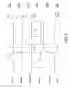
BACKGROUND OF THE INVENTIONIn a liquid crystal display comprising a plurality of gate lines and data lines, and an array of pixels arranged between adjacent gates lines and data lines, it is desirable to maintain the voltage potential on a pixel (m, n) over a reasonable period of time after the signal at the gate-line has changed from an H-state (Vgh) to an L-state (Vgl). The voltage potential is maintained by the charge capacity of each pixel. The charge is partially stored in the liquid crystal layer between the pixel electrodes, one of which is connected to a common electrode and the other is connected to the data line n through a switching element. As shown in FIG. 1, the charge capacity associated with the liquid crystal layer is represented by Clc, and the switching element is a TFT. In order to increase the charge storage capacity, a charge storage capacitor Cst is connected in parallel to the electrodes and another capacitor Cgs is connected in parallel to the TFT.
As the signal at the gate-line m changes from Vgh to Vgl, the drop in the voltage potential across the storage capacitor Cgs causes the voltage potential in the pixel relative to the common electrode to reduce by an amount of
ΔVf=Cgs(Vgh−Vgl)/(Cgs+Clc+Cst). (1)
The drop in the voltage potential in the pixel, as illustrated in FIG. 2, is known as the feed-through potential drop. The feed-through potential drop significantly affects the contrast in a black-and-white (B/W) LCD device and the shape of the gamma curve in a color LCD device.
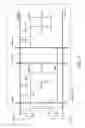
In prior art, a different shape of the gate line signal is used to compensate for the drop in the voltage potential. As shown in FIG. 3, one end of the storage capacitor Cst is connected to an adjacent gate-line m−1, instead of the common line. Furthermore, the signal on the gate lines has three voltage levels Vgh, Vgc and Vgl, as shown in FIG. 4, instead of two levels Vgh and Vgl. When the signal on the gate line m+1 is changed from Vgl to Vgh, the signal on the gate line m−1 is changed from Vgc to Vgl. As a result, the voltage potential in pixel (m, n) is pulled upward in a first step. When the signal on the gate-line m is changed from Vgc to Vgl, the voltage potential at pixel (m, n) is further pulled upward in a second step. As such, the feed-through potential drop can be partially compensated. In such a scheme, Vgc is determined by Vgh, Vgl, Cst and Cgs as follows:
(Vgc−Vgl)Cst=(Vgl−Vgh)Cgs (2)
This three-step gate-line signal is useful only when the storage capacitors Cst are tied to the gate lines, but it cannot be used when the storage capacitors Cst are tied to the common lines.
SUMMARY OF THE INVENTIONIn a liquid crystal display (LCD) panel having a plurality of pixels, each having a first electrode connected to a common line, a second electrode connected to a data line through an TFT and a charge storage capacitor connected to the second electrode at the first capacitor end, the voltage applied to the second capacitor end is equal the voltage at the common line, or Vcom. After the gate line signal has passed, a reduction in the voltage potential between the first and second electrodes occurs. This voltage reduction is known as the feed-through potential drop. In order to compensate for this voltage potential reduction, the voltage applied to the second end of the charge storage capacitor is increased from Vcom to Vcom1 after the gate line signal has passed. This applied voltage adjustment can be achieved by using two switching elements connected to the second end of the charge storage capacitor. One switching element is activated by the gate line signal so that the applied voltage is equal to Vcom. The other switching element is activated by the next gate line signal so that the applied is increased to Vcom1.
In a large LCD panel where a gate line signal is used to activate a row of pixels from one side of the panel to the other side, it is possible that the change from Vcom to Vcom1 is made on the entire panel or only on one side of the panel. It is also possible that the change on one side of the panel is from Vcom to Vcom1 and the change on the other side of the panel is from Vcom to Vcom2. Vcom2 can be smaller or greater than Vcom1.
In a transflective LCD panel where each of the pixels has a transmission area and a reflection area and each area has a separate charge storage capacitor, a similar Vcom change is applied to the charge storage capacitor associated with the transmission area and the charge storage capacitor associated with the reflection area. Likewise, in a color LCD panel where each of the pixels has three color sub-pixels and each sub-pixel has a separate charge storage capacitor, a similar Vcom change is applied to each of the charge storage capacitors in the pixel.
Furthermore, Vcom1 can be adjusted according to the temperature of the LCD panel.
The present invention will become apparent upon reading the description taken in conjunction with FIGS. 5-13.
BRIEF DESCRIPTION OF THE DRAWINGSFIG. 1 is an equivalent circuit showing various electrical components in a pixel in a prior art LCD device.
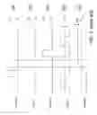
FIGS. 2a-2e show the signal levels in a pixel as shown in FIG. 1, wherein FIG. 2a is a timing diagram showing the signal level at a gate line m−1;
FIG. 2b is a timing diagram showing the signal level at a gate line m;
FIG. 2c is a timing diagram showing the signal level at a gate line m+1;
FIG. 2d is a timing diagram showing the signal level at a data line n;
FIG. 2e is a timing diagram showing the voltage level of a pixel (n, m).
FIG. 3 is an equivalent circuit showing various electrical components in a pixel in another prior art LCD device.
FIGS. 4a-4e show the signal levels in a pixel as shown in FIG. 3, wherein FIG. 4a is a timing diagram showing the signal level at a gate line m−1;
FIG. 4b is a timing diagram showing the signal level at a gate line m;
FIG. 4c is a timing diagram showing the signal level at a gate line m+1;
FIG. 4d is a timing diagram showing the signal level at a data line n;
FIG. 4e is a timing diagram showing the voltage level of a pixel (n, m).
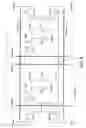
FIG. 5 is an equivalent circuit showing various electrical components in a plurality of pixels in an LCD device, according to one embodiment of the present invention.
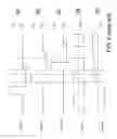
FIGS. 6a-6f show the signal levels in a pixel as shown in FIG. 5, wherein FIG. 6a is a timing diagram showing the signal level at a gate line m−1;
FIG. 6b is a timing diagram showing the signal level at a gate line m;
FIG. 6c is a timing diagram showing the signal level at a gate line m+1;
FIG. 6d is a timing diagram showing the signal level at a data line n;
FIG. 6e is a timing diagram showing the voltage level of a pixel (n, m).
FIG. 6f is a timing diagram showing the voltage level at a charge storage capacitor in the pixel.
FIG. 7 is an equivalent circuit showing various electrical components in a plurality of pixels in an LCD device, according to another embodiment of the present invention.
FIG. 8 is an equivalent circuit showing various electrical components in a plurality of pixels in an LCD device, according to yet another embodiment of the present invention.
FIG. 9 is an equivalent circuit showing various electrical components in a plurality of pixels in an LCD device, according to a different embodiment of the present invention.
FIG. 10 is an equivalent circuit showing various electrical components in a plurality of pixels in an LCD device, according to another different embodiment of the present invention.
FIG. 11 is an equivalent circuit showing various electrical components in a plurality of color sub-pixels in an LCD device, according to the present invention.
FIG. 12 is an equivalent circuit showing various electrical components in a plurality of pixels in a transflective LCD device, according to the present invention.
FIG. 13 is schematic representation showing the voltage application on the electrodes in a pixel in a LCD panel.
DETAILED DESCRIPTION OF THE INVENTION The present invention makes use of different signal levels in the common line voltages to compensate for the feed-through potential drop. As with prior art, the voltage potential associated with the charge capacity Clc is determined by the pixel voltage Vpixel and the signal level Vcom at a common line. In contrast to prior art, the voltage on one end of the additional charge storage capacitor Cst is switched between Vcom and Vcom1 as shown in FIG. 5. In one embodiment of the present invention, these voltage levels are controlled by TFT A and TFT B before the signal line VCst enters the active area of the LCD device. As shown in FIG. 6, when the signal level at gate line m is high (gate line m+1 being at Vgl), the switching TFT A and TFT are in the “ON” state but TFT B is “OFF”. The voltage potential across Clc is (Vdata−Vcom) and the voltage across Cst is also (Vdata−Vcom). The voltage potential across Cgs is (Vdata−Vgh). The total charge on these capacitors is
Qpixel=(Clc+Cst)(Vdata−Vcom)+Cgs(Vdata−Vgh). (3)
After the signal level at gate line m is changed from Vgh to Vgl but before the signal level at gate line m+1 becomes Vgh, the voltage potential across Clc and Cst is (Clc+Cst) (Vdata−ΔVf−Vcom) and the voltage potential across Cgs is (Vdata−ΔVf−Vgl). Th total charge on these capacitors is
Qpixel=(Clc+Cst)(Vdata−ΔVf−Vcom)+Cgs(Vdata−ΔVf−Vgl). (4)
By comparing Equation 3 with Equation 4, we have the feed-through potential drop ΔVf as shown in Equation 1:
Cgs(Vgl−Vgh)=(Clc+Cst+Cgs)(−ΔVf)
or
ΔVf=Cgs(Vgh−Vgl)/(Clc+Cst+Cgs). (5)
When the signal level at gate line m+1 is Vgh, the switching TFT B is “ON”. The voltage VCst is Vcom1 and the total charge after charging is
Qpixel=Cst(Vpixel−Vcom1)+Clc(Vpixel−Vcom)+Cgs(Vpixel−Vgl). (6)
In order to compensate for the feed-through potential drop, we have Vpixel=Vdata. By comparing Equations 3 and 6, we have
Cst(−Vcom1)+Cgs(−Vgl)=Cst(−Vcom)+Cgs(−Vgh)
or
Vcom1=Vcom+(Cgs/Cst)(Vgh−Vgl). (7)
The signal levels at various components associated with the pixel (m, n) are shown in FIG. 6. In particular, the signal level (Vpixel) common to Cgs, Clc and Cst is shown in FIG. 6e. As shown, the voltage level after the voltage VCst is changed from Vcom to Vcom1, Vpixel is increased until the charges on various capacitors become equilibrium.
This exemplary embodiment demonstrates that it is possible to apply different common line voltages to the charge storage capacitor in order to improve the performance of an LCD device by reducing the effect of feed-through potential drop.
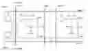
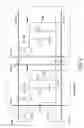
In a large area LCD device, sometimes the feed-through potential drop on the right side is different from the feed-through potential drop on the left side. It is possible to use different common line voltages on different sides of the device. For example, the compensation for the feed-through potential drop is realized only on the left side of the LCD device, as shown in FIG. 7. As shown, the switching between Vcom and Vcom1 is applied only to the pixels on the left side of the LCD device. On the right side of the LCD device, both Clc and Cst are associated with Vcom as in prior art.
In another embodiment as shown in FIG. 8, the common line voltage on the left side is switched between Vcom and Vcom1 through the control of TFT A and TFT B, but the common line voltage on the right side is switched between Vcom and Vcom2 through the control of TFT C and TFT D.
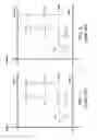
In yet another embodiment of the present invention, instead of using one charge storage capacitor Cst as shown in FIG. 5, two charge storage capacitors Cst1 and Cst2 are used in a pixel. As shown in FIG. 9, while the connection of Cst1 is the same as FIG. 5, Cst2 is connected to the gate line m+1. As such, after the signal level at gate line m+1 is changed from Vgl to Vgh, the feed-through potential drop is reduced by both the voltage change on Cst1 from Vcom to Vcom1, and the voltage change on Cst2 from Vgl to Vgh.
In a different embodiment of the present invention, instead of a constant voltage level Vcom1, a variable Vcom1 is used. As shown in FIG. 10, a temperature sensor is used to change the signal level of Vcom1 through a voltage modulator. In general, when ambient temperature changes, the liquid crystal efficiency will also change. In order to maintain the same efficiency, the driver voltage on the liquid crystal can be adjusted. When the temperature sensor detects a change in the ambient temperature, it passes information to the voltage modulator, which will look up a value to adjust the driver voltage accordingly.
It should be appreciated that the embodiments, as shown in FIGS. 5 and 7-10, can be used in a black-and-white LCD device as well as a color LCD device. For example, in a color LCD device where a pixel is divided into three color sub-pixels R, G and B, the switching between Vcom and Vcom1 is applied to the charge storage capacitors Cstr, Cstg and Cstb in different sub-pixels, as shown in FIG. 11. In general, the storage capacitors Cstr, Cstg and Cstb are designed to have different values from each other. As such, the voltage potential at each of the color sub-pixel can be compensated differently. The differences in the pixel potential among Cstr, Cstg and Cstb are designed according to gamma curve requirement. Furthermore, the switching between Vcom and Vcom1 can also be applied to a transflective LCD where a pixel is divided into a transmissive area and a reflective area. As is known in the art, the transmissive area has a transmissive electrode and the reflective area has a separate reflective electrode. As shown in FIG. 12, the charge capacity associated with the transmissive electrode is represented by CT and the charge capacity associated with the reflective electrode is CR. Each of the areas has its own TFT, Cgs and Cst. Here the subscripts 1 and 2 represent the transmissive area and the reflective area, respectively.
It should also be appreciated that, in FIGS. 5 and 7-11, Clc is the capacitance associated with the liquid crystal layer between two electrodes as shown in FIG. 13. As shown in FIG. 13, a pixel (m, n) comprises a first electrode and a second electrode. This pixel (m, n) is representative of that shown in FIG. 5. As shown, the first electrode is connected to Vcom and the second electrode is connected to switching element TFT, capacitor Cgs and capacitor Cst.
In sum, the present invention uses different values of Vcom at different signal stages in order to reduce the effect of feed-through potential drops. The switching between different Vcom values can be applied to charge storage capacitors in all or some of the pixels in the active area of a LCD device.
Thus, although the invention has been described with respect to one or more embodiments thereof, it will be understood by those skilled in the art that the foregoing and various other changes, omissions and deviations in the form and detail thereof may be made without departing from the scope of this invention.
Claims
What is claimed is:1. A method to reduce a drop in a voltage potential in a liquid crystal display having a plurality of gate lines for providing gate line signals and a plurality of data lines for providing data signals, the liquid crystal display having a plurality of pixels arranged in a plurality of pixel rows, each pixel having
a first electrode,
a second electrode, and
a liquid crystal layer segment disposed between the first and second electrodes, the first electrode electrically connected to a first voltage and the second electrode electrically connected to a data line through a switching element for receiving a data signal during a gate line signal so as to achieve the voltage potential across the liquid crystal layer segment, the pixel further comprising a charge storage capacitor having a first capacitor end and a second capacitor end, the first capacitor end of the charge storage capacitor electrically connected to the second electrode, said method comprising the steps of:
applying a second voltage to the second capacitor end of the charge storage capacitor during the gate line signal; and
applying a third voltage to the second capacitor end of the charge storage capacitor after the gate line signal has passed, wherein the third voltage in at least some of the plurality of pixels is greater than the second voltage.
2. The method of claim 1, wherein each of the pixel rows has a first side and an opposing second side and said some of the plurality of pixels are located on the first side, and some other of the plurality of pixels are located on the second side, and wherein the second voltage is substantially equal to the first voltage.
3. The method of claim 2, wherein the third voltage in said some other pixels is substantially equal to the second voltage.
4. The method of claim 2, wherein the third voltage in said some other pixels is also greater than the second voltage.
5. The method of claim 2, wherein the third voltage in said some other pixels is different from the third voltage in said some pixels.
6. The method of claim 1, wherein the plurality of pixel rows include a pixel row m and an adjacent pixel row m+1, and the plurality of gate lines include a gate line m for driving the pixel row m and a gate line m for driving the pixel row m+1 and wherein
the gate line signal is provided to the gate line m for driving the pixel row m,
a next gate line signal is provided to the gate line m+1 for driving the pixel row m+1, and
the third voltage is applied to the second capacitor end of the charge storage capacitor during the next gate line signal.
7. The method of claim 6, wherein each pixel further comprises a further charge storage capacitor, the further charge storage capacitor having a first capacitor end and a second capacitor end, the first capacitor end electrically connected to the second electrode, the second capacitor end electrically connected to the gate line m+1.
8. The method of claim 4, wherein the third voltage varies with temperature of the liquid crystal display.
9. The method of claim 2, wherein the liquid crystal display is a transflective display and each pixel has a transmission sub-pixel and a reflective sub-pixel, the second electrode comprising a transmissive electrode in the transmission sub-pixel, the reflective sub-pixel having a third electrode electrically connected to the data line through another switching element for receiving the data signal during the gate line signal, the reflective sub-pixel further comprising a further charge storage capacitor having a first capacitor end and a second capacitor end, the first capacitor end electrically connected to the third electrode, said method further comprising the step of:
applying the third voltage to the second capacitor end of the further charge storage capacitor.
10. The method of claim 2, wherein the liquid crystal display is a color display and each pixel has a first color sub-pixel, a second color sub-pixel and a third color sub-pixel, and wherein the second electrode comprises a first sub-electrode in the first color sub-pixel, a second sub-electrode in the second color sub-pixel and a third sub-electrode in the third color sub-pixel, the first sub-electrode electrically connected to the first end of the charge storage capacitor, wherein
the second color sub-pixel further comprises a second charge storage capacitor having a first capacitor end and a second capacitor end, the first capacitor end electrically connected to the second sub-electrode, and
the third color sub-pixel further comprises a third charge storage capacitor having a first capacitor end and a second capacitor end, the first capacitor end electrically connected to the third sub-electrode, said method further comprising the step of:
applying the third voltage to the second capacitor end of the second charge storage capacitor and the second capacitor end of the third charge storage capacitor.
11. A liquid crystal display having a plurality of pixels arranged in a plurality of pixel rows, a plurality of gate lines for providing gate line signals and a plurality of data lines for providing data signals to the plurality of pixels, each pixel having
a switching element;
a first electrode,
a second electrode,
a liquid crystal layer segment disposed between the first and second electrodes, the first electrode electrically connected to a first voltage and the second electrode electrically connected to a data line through the switching element for receiving a data signal during a gate line signal, and
a charge storage capacitor having a first capacitor end and a second capacitor end, the first capacitor end electrically connected to the second electrode, said liquid crystal display comprising:
a voltage source connected to the second capacitor end of the charge storage capacitor so as to apply the first voltage to the charge storage capacitor during the gate line signal and to apply a second voltage to the charge storage capacitor after the gate line signal has passed, wherein the second voltage in at least some of the plurality of pixels is greater than the second voltage.
12. The liquid crystal display of claim 11, wherein each of the pixel rows has a first side and an opposing second side, and said some of the plurality of pixels are located on the first side and some other of the plurality of pixels are located on the second side.
13. The liquid crystal display of claim 12, wherein the second voltage in said some other pixels is substantially equal to the first voltage.
14. The liquid crystal display of claim 12, wherein the second voltage in said some other pixels is also greater than the first voltage.
15. The liquid crystal display of claim 12, wherein the second voltage in said some pixels is different from the second voltage in said some other pixels.
16. The liquid crystal display of claim 11, wherein the plurality of pixel rows include a pixel row m and an adjacent pixel row m+1 and the plurality of gate lines include a gate line m for driving the pixel row m and a gate line m for driving the pixel row m+1 and wherein
the gate line signal is provided to the gate line m for driving the pixel row m,
a next gate line signal is provided to the gate line m+1 for driving the pixel row m+1, and
the second voltage is applied to the second capacitor end of the charge storage capacitor during the next gate line signal.
17. The liquid crystal display of claim 16, wherein each pixel further comprises a further storage capacitor, the further charge storage capacitor having a first capacitor end and a second capacitor end, the first capacitor end electrically connected to the second electrode, the second capacitor end electrically connected to the gate line m+1.
18. The liquid crystal display of claim 14, further comprising a temperature sensor operatively connected to the voltage source, the temperature sensor adapted to sense a temperature of the liquid crystal display for providing a signal indicative of the sensed temperature, so as to change the second voltage at least based on the sensed temperature.
19. The liquid crystal of claim 12, wherein each pixel has a transmission sub-pixel and a reflective sub-pixel, and wherein
the second electrode comprises a transmissive electrode in the transmission sub-pixel, and
the reflective sub-pixel comprises a third electrode electrically connected to the data line through another switching element for receiving the data signal during the gate line signal, the reflective sub-pixel further comprising a further charge storage capacitor having a first capacitor end and a second capacitor end, the first capacitor end electrically connected to the third electrode, and wherein the second voltage is also applied to the second capacitor end of the further charge storage capacitor.
20. The liquid crystal display of claim 12, wherein each pixel has a first color sub-pixel, a second color sub-pixel and a third color sub-pixel, and wherein the second electrode comprises a first sub-electrode in the first color sub-pixel, a second sub-electrode in the second color sub-pixel and a third sub-electrode in the third color sub-pixel, the first sub-electrode electrically connected to the first end of the charge storage capacitor, wherein
the second color sub-pixel further comprises a second charge storage capacitor having a first capacitor end and a second capacitor end, the first capacitor end electrically connected to the second sub-electrode, and
the third color sub-pixel further comprises a third charge storage capacitor having a first capacitor end and a second capacitor end, the first capacitor end electrically connected to the third sub-electrode, and wherein the second voltage is also applied to the second capacitor end of the second charge storage capacitor and the second capacitor end of the third charge storage capacitor.
Images & Drawings included:


Sources:
- United States Patent and Trademark Office - verify current appl. status at the USPTO↗
Recent applications in this class:
- » 20250014532 2025-01-09
METHOD FOR DRIVING LIQUID CRYSTAL DISPLAY DEVICE - » 20240404486 2024-12-05
LIQUID CRYSTAL DISPLAY DEVICE AND METHOD OF DRIVING THE SAME - » 20240404485 2024-12-05
LIQUID CRYSTAL DISPLAY DEVICE AND METHOD OF DRIVING THE SAME - » 20240296807 2024-09-05
DISPLAY DEVICE - » 20240257780 2024-08-01
Display device - » 20240087542 2024-03-14
Driving method and driving circuit of display panel, and display device - » 20240062733 2024-02-22
Display device - » 20240021171 2024-01-18
Display device - » 20230036780 2023-02-02
Driving circuit, multi-stage driving circuit and display panel - » 20220310029 2022-09-29
SENSOR-EQUIPPED DISPLAY DEVICE
Recent applications for this Assignee:
- » 20230262206 2023-08-17
Naked-eye stereoscopic display system and display method thereof - » 20230253379 2023-08-10
Display apparatus - » 20230234055 2023-07-27
OPTOELECTRONIC TWEEZER DEVICE AND FABRICATION METHOD THEREOF - » 20230223674 2023-07-13
Antenna module and display apparatus - » 20230197917 2023-06-22
DISPLAY APPARATUS - » 20230187457 2023-06-15
Display panel - » 20230187417 2023-06-15
Display panel including opaque encapsulation and doped planarization layers and manufacturing method thereof - » 20230143881 2023-05-11
Display panel - » 20230140381 2023-05-04
Stretchable display panel - » 20230137029 2023-05-04
PHOTOSENSITIVE DEVICE