Housing and method for making the same
US20060286392A1
2006-12-21
11/396,838
2006-04-03
Abstract:
A housing (100) includes a housing base (10), a chromium film (12), and a chromium carbide film (14). The housing base is made of a material of metal or metal alloys. The chromium film is formed on a surface of the housing base, and the chromium carbide film is formed on a surface of the chromium film. The present invention also provides a method for making the housing.
Inventors:
- XIAN-FENG LUO 3 🇨🇳 Shenzhen, China
- Chih-Pen Lin 4 🇹🇼 Tu-Cheng, Taiwan
- Yong-Ming Li 2 🇨🇳 Shenzhen, China
- Yi-Lin Zhang 2 🇨🇳 Shenzhen, China
- Cheng-Guo Zhang 1 🇨🇳 Shenzhen, China
- Nai-Juan Ren 1 🇨🇳 Shenzhen, China
Assignee:
- FIH CO., LTD 62 🇹🇼 Shindian City, Taiwan
Interested in similar patents?
Get notified when new applications in this technology area are published.
Classification:
C23C14/165 » CPC main
Coating by vacuum evaporation, by sputtering or by ion implantation of the coating forming material characterised by the coating material; Metallic material, boron or silicon on metallic substrates or on substrates of boron or silicon by cathodic sputtering
B32B15/01 » CPC further
Layered products comprising a layer of metal all layers being exclusively metallic
B32B15/013 » CPC further
Layered products comprising a layer of metal all layers being exclusively metallic one layer being formed of an iron alloy or steel, another layer being formed of a metal other than iron or aluminium
B32B15/017 » CPC further
Layered products comprising a layer of metal all layers being exclusively metallic one layer being formed of aluminium or an aluminium alloy, another layer being formed of an alloy based on a non ferrous metal other than aluminium
C23C14/0635 » CPC further
Coating by vacuum evaporation, by sputtering or by ion implantation of the coating forming material characterised by the coating material Carbides
C23C28/322 » CPC further
Coating for obtaining at least two superposed coatings either by methods not provided for in a single one of groups - or by combinations of methods provided for in subclasses and or; Coatings combining at least one metallic layer and at least one inorganic non-metallic layer including at least one pure metallic layer only coatings of metal elements only
C23C28/341 » CPC further
Coating for obtaining at least two superposed coatings either by methods not provided for in a single one of groups - or by combinations of methods provided for in subclasses and or; Coatings combining at least one metallic layer and at least one inorganic non-metallic layer including at least one inorganic non-metallic material layer, e.g. metal carbide, nitride, boride, silicide layer and their mixtures, enamels, phosphates and sulphates with at least one carbide layer
G06F1/1613 » CPC further
Details not covered by groups - and; Constructional details or arrangements for portable computers
G06F1/1684 » CPC further
Details not covered by groups - and; Constructional details or arrangements for portable computers; Constructional details or arrangements of portable computers not specific to the type of enclosures covered by groups - Constructional details or arrangements related to integrated I/O peripherals not covered by groups -
G06F1/181 » CPC further
Details not covered by groups - and; Constructional details or arrangements; Packaging or power distribution Enclosures
H05K5/02 » CPC further
Casings, cabinets or drawers for electric apparatus Details
H05K5/02 » CPC further
Casings, cabinets or drawers for electric apparatus Details
Y10T428/12576 » CPC further
Stock material or miscellaneous articles; All metal or with adjacent metals; Composite; i.e., plural, adjacent, spatially distinct metal components [e.g., layers, joint, etc.] with additional, spatially distinct nonmetal component Boride, carbide or nitride component
Y10T428/31678 » CPC further
Stock material or miscellaneous articles; Composite [nonstructural laminate] Of metal
B32B15/04 IPC
Layered products comprising a layer of metal comprising metal as the main or only constituent of a layer, next to another layer of a
B32B9/00 IPC
Layered products characterised by particular substances used
B32B9/00 IPC
Layered products comprising a layer of a particular substance not covered by groups -
C23C14/00 IPC
Coating by vacuum evaporation, by sputtering or by ion implantation of the coating forming material
Description
BACKGROUND OF THE INVENTION1. Field of the Invention
The present invention generally relates to portable devices and, more particularly, to a housing for a portable device and a method for making the housing.
2. Discussion of the Related Art
With the development of wireless communication and information processing technologies, portable electronic devices such as notebook computers, mobile phones, digital cameras, and personal digital assistants (PDAs) are now in widespread use. These electronic devices enable consumers to enjoy high technology services anytime and anywhere.
The portable electronic device should have a hard housing for protecting internal elements received therein. A conventional housing for a portable electronic device is made of plastic material, such as acrylonitrile-butadiene-styrene (ABS). Nowadays, housings made of metal or metal alloys, such as stainless steel, aluminum and its alloys, magnesium and its alloys, and titanium and its alloys, are used for the portable electronic devices.
Housings made of stainless steel, aluminum alloy, and aluminum-magnesium alloy may easily be scratched or damaged in daily use, since these materials are relatively soft compared to other metals. Thus, the appearance and attractiveness of the housing can easily be blemished by being scratched or by other damage. Titanium alloy has good hardness, however, the high price of titanium makes it prohibitively expensive for use in portable electronic devices.
Various methods have been devised for treating stainless steel to increase its hardness, including, e.g. nitridation and carburization. In nitridation, the surface of the stainless steel is hardened by forming nitrides. This is done by introducing nitrogen into the stainless steel, usually by heating the stainless steel in gaseous ammonia. In carburization, the outer layer of low-carbon stainless steel is converted into high-carbon stainless steel by contact with a carbonaceous material. Both nitridation and carburization can considerably increase the surface hardness of stainless steel. By carburization, the surface hardness of the treated stainless steel can reach around 800 HV. Whereas by nitridation, a surface hardness of around 600 HV can be reached. Both processes, however, require high temperature treatments for a long period of time. For example, nitridation has to be carried out at a temperature of 524-549° C., and the process takes from 24 to 48 hours to complete. For carburization, the temperature is even higher, with temperatures up to 1,000° C., and takes about 20 hours to complete the process. Therefore, nitridation and carburization have prohibitively low productivity and efficiency, and thus increase the cost of portable electronic device to an unacceptable degree.
In addition, for such metals and metal alloys as aluminum, aluminum alloys, magnesium, magnesium alloys, titanium, and titanium alloys, as these have little or no chromium, neither nitridation nor carburization of a housing made of such material is possible. Metallic hard chromium electroplating is difficult to apply to aluminum and its alloys, magnesium and its alloys, and titanium and its alloys, because these materials oxidize rapidly in electrolytic solutions, and become electrically un-conductive, thus preventing electroplating.
Therefore, a housing which has a high hardness, is desired in order to overcome the above-described problems.
SUMMARY OF THE INVENTIONIn one aspect, a housing includes a housing base, a chromium film, and a chromium carbide film. The housing base is made of metal or metal alloys. The chromium film is formed on a surface of the housing base, and the chromium carbide film is formed on a surface of the chromium film.
In another aspect, a method for making a housing includes the steps of: providing a housing base made of metal or metal alloys; forming a chromium film on a surface of the housing base, and forming a chromium carbide film on a surface of the chromium film.
Other advantages and novel features will become more apparent from the following detailed description when taken in conjunction with the accompanying drawings.
BRIEF DESCRIPTION OF THE DRAWINGSMany aspects of the housing can be better understood with reference to the following drawings. The components in the drawings are not necessarily drawn to scale, the emphasis instead being placed upon clearly illustrating the principles of the present housing. Moreover, in the drawings, like reference numerals designate corresponding parts throughout the several views.
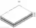
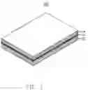
FIG. 1 is a schematic view of a housing in accordance with a preferred embodiment.
DETAILED DESCRIPTION OF THE EMBODIMENTSReferring to FIG. 1, showing a portion of a housing 100 in a preferred embodiment, the housing 100 includes a housing base 10, a chromium film 12, and a chromium carbide film 14. The housing base 10 is made of metal or metal alloys, such as stainless steel, aluminum, aluminum alloys, magnesium, magnesium alloys, titanium, and titanium alloys. The chromium film 12 is formed on a surface of the housing base 10, and the chromium carbide film 14 is formed on a surface of the chromium film 12.
The chromium film 12 has an approximate thickness in the range of 0.6-0.8 micron. The chromium carbide film 14 has an approximate thickness in the range of 1.0-2.0 micron. In the chromium carbide film 14, the atom ratio of carbon and chromium is preferably in the range of 0.4-0.5.
The chromium film 12 and the chromium carbide film 14 are formed to improve the surface hardness of the housing 100. The chromium film 12 and the chromium carbide film 14 are both very hard, thus their application increases the surface hardness of the housing 100 by up to 600 HV. The chromium film 12 helps the chromium carbide film 14 adhere to the housing base 10. Furthermore, the chromium film 12 and the chromium carbide film 14 have a stainless-steel-like appearance, which gives the housing 100 an attractive surface appearance.
An exemplary method for making the housing 100 is provided. Firstly, a housing base 10 made of metal or metal alloys is formed by die molding or stamp molding. The metal or metal alloys can be stainless steel, aluminum, aluminum alloys, magnesium, magnesium alloys, titanium, and titanium alloys. Secondly, a chromium film 12 is deposited on the surface of the housing base 10 by sputtering. During sputtering, a chromium metal is used as the sputtering target, and an inert gas is used as the sputtering gas. Thirdly, a chromium carbide film 14 is deposited on the surface of the chromium film 12 by sputtering, this time using a hydrocarbon gas as the sputtering gas. Thereby, a housing 100 is obtained.
The housing 100 can be used in any portable device, such as a cover of a portable electronic device, a watch band/case, or spectacle-frames.
It is believed that the present embodiments and their advantages will be understood from the foregoing description, and it will be apparent that various changes may be made thereto without departing from the spirit and scope of the invention or sacrificing all of its material advantages, the examples herebefore described merely being preferred or exemplary embodiments of the invention.
Claims
What is claimed is:1. A housing comprising:
a housing base;
a chromium film formed on a surface of the housing base; and
a chromium carbide film formed on a surface of the chromium film.
2. The housing as claimed in claim 1, wherein the housing base is made of a metal or metal alloy.
3. The housing as claimed in claim 2, wherein the metal or alloy is selected from the group consisting of stainless steel, aluminum, aluminum alloys, magnesium, magnesium alloys, titanium, and titanium alloys.
4. The housing as claimed in claim 1, wherein the chromium film has an approximate thickness in the range of 0.6-0.8 micron.
5. The housing as claimed in claim 1, wherein the chromium carbide film has an approximate thickness in the range of 1.0-2.0 micron.
6. The housing as claimed in claim 5, wherein an atom ratio of carbon and chromium in the chromium carbide film is in the range of 0.4-0.5.
7. A method for making a housing, comprising the steps of:
providing a housing base;
forming a chromium film on a surface of the housing base; and
forming a chromium carbide film on a surface of the chromium film.
8. The method as claimed in claim 7, the housing base is made of a metal or metal alloy.
9. The method as claimed in claim 8, wherein the metal or metal alloys are selected from the group consisting of stainless steel, aluminum, aluminum alloys, magnesium, magnesium alloys, titanium, and titanium alloys.
10. The method as claimed in claim 7, wherein the chromium film is formed by sputtering, a chromium target is used as the sputtering target.
11. The method as claimed in claim 7, wherein the chromium carbide film is formed by sputtering, a chromium target is used as the sputtering target, and a hydrocarbon gas is used as the sputtering gas.
12. The method as claimed in claim 11, wherein the hydrocarbon gas is one of methane, ethane, and propane.
13. The method as claimed in claim 7, wherein the chromium film has an approximate thickness in the range of 0.6-0.8 micron, the chromium carbide film has an approximate thickness in the range of 1.0-2.0 micron.
14. The method as claimed in claim 13, wherein an atom ratio of carbon and chromium in the chromium carbide film is in the range of 0.4-0.5.
Images & Drawings included:
Sources:
- United States Patent and Trademark Office - verify current appl. status at the USPTO↗
Similar patent applications:
- » 20090092838
Housing, injection mold for making the housing, and method for making the housing by using the injection mold - » 20100279073
Housing for electronic device, mold for making the housing, and method for making the housing - » 20090045533
MOLD FOR MAKING A HOUSING AND METHOD FOR MAKING THE HOUSING - » 20100097276
HOUSING, METHOD OF MAKING THE HOUSING, AND ELECTRONIC DEVICE USING THE HOUSING - » 20130288043
HOUSING AND METHOD FOR MAKING HOUSING - » 20130141885
HOUSING AND METHOD FOR MAKING HOUSING - » 20090009942
Housing for electronic devices, electronic device using the housing and method for making the housing - » 20100068465
HOUSING AND METHOD FOR MAKING THE HOUSING - » 20090009941
HOUSING FOR AN ELECTRONIC DEVICE, ELECTRONIC DEVICE USING THE HOUSING, AND METHOD FOR MAKING THE HOUSING - » 20100288357
HOUSING, ELECTRONIC DEVICE USING THE HOUSING, AND METHOD FOR MAKING THE HOUSING
Recent applications in this class:
- » 20250101570 2025-03-27
DEPOSITION MASK AND METHOD FOR MANUFACTURING THE SAME - » 20250092506 2025-03-20
PVD Deposited Ternary and Quaternary NiTi Alloys and Methods of Making Same - » 20250084523 2025-03-13
PVD Deposited Ternary and Quaternary NiTi Alloys and Methods of Making Same - » 20240158907 2024-05-16
NANO-TWINNED ULTRA-THIN METALLIC FILM STRUCTURE AND METHODS FOR FORMING THE SAME - » 20230304139 2023-09-28
METHODS FOR APPLYING DECORATIVE METAL FILMS ON POLYMERIC SURFACES - » 20230100972 2023-03-30
Method for producing a coating of a base body and functional element having a base body with a coating - » 20230032964 2023-02-02
METHOD OF ION-PLASMA APPLICATION OF CORROSION-RESISTANT FILM COATINGS ON ARTICLES MADE FROM ZIRCONIUM ALLOYS - » 20230019656 2023-01-19
Sputtering target - » 20220372611 2022-11-24
PVD deposited ternary and quaternary NiTi alloys and methods of making same - » 20220372610 2022-11-24
Engineered multi-dimensional metallurgical properties in PVD materials
Recent applications for this Assignee:
- » 20070077972 2007-04-05
Hinge assembly for a foldable electronic device - » 20070077971 2007-04-05
Hinge assembly for a foldable electronic device - » 20070064381 2007-03-22
Foldable electronic device - » 20070058328 2007-03-15
Slide mechanism for a slide-type portable terminal device - » 20070039833 2007-02-22
Method for measuring corrosion inhibitor concentration - » 20070037431 2007-02-15
Surface contact card holder - » 20070036351 2007-02-15
Housing for an electronic device, and method for making the same - » 20070034530 2007-02-15
Method for measuring metal ion concentration - » 20070033816 2007-02-15
Rapid workpiece engraving apparatus - » 20070026297 2007-02-01
Battery cover latching mechanism for portable electronic device