Power semiconductor device
US20060286732A1
2006-12-21
11/449,940
2006-06-09
✅ Patent granted
US 7,385,273 B2
2008-06-10
-
-
Steven Loke | Tram H Nguyen
2026-06-09
Abstract:
A power semiconductor device that includes a plurality of gate structure each having a gate insulation of a first thickness, and a termination region, the termination including a field insulation body surrounding the active region and having a recess that includes a bottom insulation thicker than the first thickness.
Inventors:
- Hugo R.G. Burke 4 🇬🇧 PontyClun, United Kingdom
- Simon Green 2 🇬🇧 Cardiff, United Kingdom
- Hugo R Burke 1 🇬🇧 Pontyclun, United Kingdom
Assignee:
- INTERNATIONAL RECTIFIER CORPORATION 879 🇺🇸 EL SEGUNDO, CA, United States
Interested in similar patents?
Get notified when new applications in this technology area are published.
Classification:
H01L31/113 IPC
Semiconductor devices sensitive to infra-red radiation, light, electromagnetic radiation of shorter wavelength or corpuscular radiation and specially adapted either for the conversion of the energy of such radiation into electrical energy or for the control of electrical energy by such radiation; Processes or apparatus specially adapted for the manufacture or treatment thereof or of parts thereof; Details thereof in which radiation controls flow of current through the device, e.g. photoresistors characterised by at least one potential-jump barrier or surface barrier, e.g. phototransistors; Devices sensitive to infra-red, visible or ultra-violet radiation characterised by field-effect operation, e.g. junction field-effect phototransistor being of the conductor-insulator-semiconductor type, e.g. metal-insulator-semiconductor field-effect transistor
H01L29/1095 » CPC further
Semiconductor devices adapted for rectifying, amplifying, oscillating or switching, or capacitors or resistors with at least one potential-jump barrier or surface barrier, e.g. PN junction depletion layer or carrier concentration layer; Details of semiconductor bodies or of electrodes thereof; Multistep manufacturing processes therefor; Semiconductor bodies ; Multistep manufacturing processes therefor characterised by their shape; characterised by the shapes, relative sizes, or dispositions of the semiconductor regions ; characterised by the concentration or distribution of impurities within semiconductor regions with semiconductor regions connected to an electrode not carrying current to be rectified, amplified or switched and such electrode being part of a semiconductor device which comprises three or more electrodes Body region, i.e. base region, of DMOS transistors or IGBTs
H01L29/402 » CPC further
Semiconductor devices adapted for rectifying, amplifying, oscillating or switching, or capacitors or resistors with at least one potential-jump barrier or surface barrier, e.g. PN junction depletion layer or carrier concentration layer; Details of semiconductor bodies or of electrodes thereof; Multistep manufacturing processes therefor; Electrodes ; Multistep manufacturing processes therefor Field plates
H01L29/408 » CPC further
Semiconductor devices adapted for rectifying, amplifying, oscillating or switching, or capacitors or resistors with at least one potential-jump barrier or surface barrier, e.g. PN junction depletion layer or carrier concentration layer; Details of semiconductor bodies or of electrodes thereof; Multistep manufacturing processes therefor; Electrodes ; Multistep manufacturing processes therefor with an insulating layer with a particular dielectric or electrostatic property, e.g. with static charges or for controlling trapped charges or moving ions, or with a plate acting on the insulator potential or the insulator charges, e.g. for controlling charges effect or potential distribution in the insulating layer, or with a semi-insulating layer contacting directly the semiconductor surface
H01L29/41766 » CPC further
Semiconductor devices adapted for rectifying, amplifying, oscillating or switching, or capacitors or resistors with at least one potential-jump barrier or surface barrier, e.g. PN junction depletion layer or carrier concentration layer; Details of semiconductor bodies or of electrodes thereof; Multistep manufacturing processes therefor; Electrodes ; Multistep manufacturing processes therefor characterised by their shape, relative sizes or dispositions carrying the current to be rectified, amplified or switched; Source or drain electrodes for field effect devices with at least part of the source or drain electrode having contact below the semiconductor surface, e.g. the source or drain electrode formed at least partially in a groove or with inclusions of conductor inside the semiconductor
G01F1/58 IPC
Measuring the volume flow or mass flow of fluid or fluent solid material wherein the fluid passes through a meter in a continuous flow by using electric or magnetic effects by electromagnetic flowmeters
H01L29/76 IPC
Semiconductor devices adapted for rectifying, amplifying, oscillating or switching, or capacitors or resistors with at least one potential-jump barrier or surface barrier, e.g. PN junction depletion layer or carrier concentration layer; Details of semiconductor bodies or of electrodes thereof; Multistep manufacturing processes therefor; Types of semiconductor device ; Multistep manufacturing processes therefor controllable by only the electric current supplied, or only the electric potential applied, to an electrode which does not carry the current to be rectified, amplified or switched Unipolar devices, e.g. field effect transistors
H01L29/94 IPC
Semiconductor devices adapted for rectifying, amplifying, oscillating or switching, or capacitors or resistors with at least one potential-jump barrier or surface barrier, e.g. PN junction depletion layer or carrier concentration layer; Details of semiconductor bodies or of electrodes thereof; Multistep manufacturing processes therefor; Types of semiconductor device ; Multistep manufacturing processes therefor controllable only by variation of the electric current supplied, or only the electric potential applied, to one or more of the electrodes carrying the current to be rectified, amplified, oscillated or switched; Capacitors with potential-jump barrier or surface barrier Metal-insulator-semiconductors, e.g. MOS
H01L31/062 IPC
Semiconductor devices sensitive to infra-red radiation, light, electromagnetic radiation of shorter wavelength or corpuscular radiation and specially adapted either for the conversion of the energy of such radiation into electrical energy or for the control of electrical energy by such radiation; Processes or apparatus specially adapted for the manufacture or treatment thereof or of parts thereof; Details thereof adapted as photovoltaic [PV] conversion devices characterised by at least one potential-jump barrier or surface barrier the potential barriers being only of the metal-insulator-semiconductor type
H01L31/119 IPC
Semiconductor devices sensitive to infra-red radiation, light, electromagnetic radiation of shorter wavelength or corpuscular radiation and specially adapted either for the conversion of the energy of such radiation into electrical energy or for the control of electrical energy by such radiation; Processes or apparatus specially adapted for the manufacture or treatment thereof or of parts thereof; Details thereof in which radiation controls flow of current through the device, e.g. photoresistors characterised by at least one potential-jump barrier or surface barrier, e.g. phototransistors; Devices sensitive to very short wavelength, e.g. X-rays, gamma-rays or corpuscular radiation characterised by field-effect operation, e.g. MIS type detectors
Description
RELATED APPLICATIONThis application is based on and claims benefit of U.S. Provisional Application Ser. No. 60/689,293, filed on Jun. 10, 2005, entitled Self Aligned Contact Improvement to Form Self Aligned Gate Contact and Save One Mask Step, to which a claim of priority is hereby made and the disclosure of which is incorporated by reference.
BACKGROUND OF THE INVENTIONThe present invention relates to power semiconductor devices and a method of fabricating a power semiconductor device.
MOSgated devices, such as power MOSFETs and IGBTs are very well known, and have a gate electrode, usually made of conductive polysilicon, which must be electrically insulated from the source electrode (or emitter electrode) and yet must be electrically connected to an external metallic gate conductor or gate pad, usually of aluminum. In a self aligned contact power MOSFET, contact to the source is made in the active area, using spacer technology. However, the gate metal-to-gate polysilicon contact at the gate pad has required the use of a separate photo mask step.
U.S. Pat. No. 6,893,923, assigned to the assignee of the present application, discloses a power MOSFET (FIG. 1) which includes a recess formed in the field oxide in the termination region thereof. The recess is formed during the active mask step in which the field oxide layer is etched to define the active area and the bottom thereof is oxidized during the gate oxidation step. Thus, the oxide in the bottom of the recess is the same thickness as the gate oxide in the device.
The present invention provides certain improvements over the process and the device disclosed in the prior art.
SUMMARY OF THE INVENTIONA power semiconductor device according to an embodiment of the present invention includes an active region having a plurality of gate structure each having a gate insulation of a first thickness, a termination region, the termination including a field insulation body surrounding the active region, the field insulation body having a recess formed therein the recess having a bottom insulation of a second thickness that is thicker than the first thickness, and a conductive body formed in the recess on the bottom insulation, and a PN region disposed under the bottom insulation.
A power MOSFET according to the preferred embodiment further includes a field plate structure adjacent the field insulation body and the active region, the field plate region including a field plate insulation body thicker than the first thickness, and a conductive field plate body disposed over the field plate insulation body.
According to an aspect of the present invention the PN region includes a region of one conductivity formed in a region of another conductivity, the region of one conductivity being disposed directly under the bottom insulation and the bottom insulation including conductive impurities of the one conductivity. Furthermore, the field plate insulation body may include conductive impurities of the one conductivity.
A method for fabricating a power semiconductor device according to the present invention may include depositing a field oxide body on a surface of a semiconductor body of a first conductivity, forming an opening in the field oxide body whereby a portion of the semiconductor body is exposed, implanting dopants of a second conductivity in the semiconductor body through the opening in the field oxide body, growing an oxide body on the semiconductor body having a first thickness, removing a portion of the field oxide body to define an active region, growing a gate oxide body over the defined active region, the gate oxide having a second thickness less than the first thickness, depositing polysilicon over the gate oxide body and inside the opening, and removing portions of the polysilicon to define a plurality of gate electrodes, and a conductive body inside the opening.
Other features and advantages of the present invention will become apparent from the following description of the invention which refers to the accompanying drawings.
BRIEF DESCRIPTION OF THE DRAWINGSFIG. 1 illustrates a power semiconductor device according to prior art.
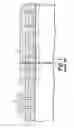
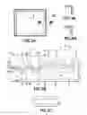
FIG. 2A schematically shows a top plan view of a power semiconductor device according to the present invention.
FIG. 2B schematically shows a cross-sectional view of a device according to the present invention along line 2B-2B in FIG. 2A viewed in the direction of the arrows.
FIG. 2C schematically illustrates an enlarged view of section 2C in FIG. 2A
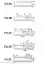
FIGS. 3A-3E illustrate a method for fabricating a power MOSFET according to the present invention.
FIGS. 4A-4B illustrate two examples regarding contact to the polysilicon band in the termination region.
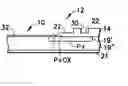
DETAILED DESCRIPTION OF EMBODIMENTS OF THE INVENTIONReferring to FIGS. 2A-2C, a power semiconductor device according to the present invention includes an active region 10 and a termination region 12. Termination region 12 includes a field insulation body 14 surrounding active region 10. Field insulation body 14 includes a recess 16 formed therein having bottom insulation 18, an electrically conductive body 20 formed over bottom insulation 18 and metallic gate runner 36 electrically connected to conductive body 20. Note that a PN junction region 19 is disposed under at least bottom insulation 18. PN junction region in the preferred embodiment includes diffusion region 19′ of preferably P type variety formed in a semiconductor body 19″ of N type variety.
A device according to the preferred embodiment further includes a field plate structure adjacent field insulation body 14 and active region 10. Field plate structure preferably includes field plate insulation body 22, and conductive field plate body 24 disposed over field plate insulation body 22. Note that in the preferred embodiment PN junction region 19 extends into active region 10 and is integrated with a base region 26 of the same conductivity. Note that in the preferred embodiment base region 26 includes source region 28 formed therein. A source electrode is ohmically connected to at least source regions 28.
Active region 10 further includes a plurality of gate structures, each including a gate insulation body 32, and a gate electrode 34 formed on gate insulation body 32. An insulation cap 33 composed preferably of silicon dioxide electrically insulates each gate electrode 34 and field plate 24.
According to one aspect of the present invention bottom insulation 18, and field plate insulation 22 are thicker than gate insulation bodies 32. Thus, for example, gate insulation bodies 32 are usually less than 1000 Å thick, while bottom insulation 18 and field plate insulation 22 may be up to 3000 Å thick or thicker insulation (but less than the thickness of field insulation body 14). Furthermore, field body 14 may be composed of field oxide (e.g. TEOS), and bottom insulation 18 and field plate insulation 22 may be composed of grown oxide, which is denser than field oxide.
According to another aspect of the present invention field plate insulation 22 and bottom insulation 18 are doped with dopants of the same polarity as region 19′. Thus, in the preferred embodiment, field plate insulation 22 and bottom insulation 18 are P type doped.
Preferably, conductive body 20, conductive field plate body 24, and gate electrodes 34 are composed of conductive polysilicon.
Referring next to FIGS. 3A-3E, a power semiconductor device according to an embodiment of the present invention is fabricated by first depositing a field insulation (oxide) body 14 over a semiconductor body 19″ of one conductivity (FIG. 3A). Semiconductor body 19″ is preferably an N type epitaxially grown silicon body on a silicon substrate 21.
Next, a first opening 38 and a second opening 40 are formed in field oxide 14, each opening exposing a portion of semiconductor body 19″ below field oxide body 14 as illustrated by FIG. 3B.
Thereafter, dopants of a conductivity opposite to that of semiconductor body 19″ (e.g. P type dopants) are implanted into semiconductor body 19″ through openings 38, 40 as illustrated again by FIG. 3B.
Next, in a thermal step, oxide is grown at the bottom of each opening 38, 40 on the exposed portions of semiconductor body 19″. During the thermal step the implanted P type dopants are driven to form region 19′. Note that the oxide grown at the bottom of opening 38 will serve as bottom insulation 18, and the oxide at the bottom of opening 40 will serve as field plate insulation 22. The structure so obtained is illustrated by FIG. 3C.
Thereafter, field oxide 14 is removed to define the area for active region 10 as shown by FIG. 3D.
Gate oxide 32 is then grown in a thermal step over the exposed portion of semiconductor body 19″. Next, polysilicon is deposited, which fills opening 38, and covers field plate insulation 22. Polysilicon is then patterned to form gate electrodes 34, field plate conductive body 24, and conductive body 20.
Conventional steps are then carried out to a device according to the present invention as illustrated above.
Note that contact may be made outside existing band 20 of polysilicon resulting in a wider region 19′ (see FIG. 4A). Alternatively, contact may be made inside of existing band 20 of polysilicon resulting in region 19′ of the same dimension, but a wider field resulting in a narrower insulation 22 down to the active region.
Although the present invention has been described in relation to particular embodiments thereof, many other variations and modifications and other uses will become apparent to those skilled in the art. It is preferred, therefore, that the present invention be limited not by the specific disclosure herein, but only by the appended claims.
Claims
What is claimed is:1. A power semiconductor device comprising:
an active region, said active region including a plurality of gate structure each having a gate insulation of a first thickness;
a termination region, said termination including a field insulation body surrounding said active region, said field insulation body having a recess formed therein said recess having a bottom insulation of a second thickness that is thicker than said first thickness;
a conductive body formed in said recess on said bottom insulation; and
a PN region disposed under said bottom insulation.
2. A power semiconductor device according to claim 1, further comprising a field plate structure adjacent said field insulation body and said active region, said field plate region including a field plate insulation body thicker than said first thickness, and a conductive field plate body disposed over said field plate insulation body.
3. A power semiconductor device according to claim 1, wherein PN region extends below said field plate structure and into said active region.
4. A power semiconductor device according to claim 3, wherein said region includes at least one source region and a source electrode ohmically connected to said source region.
5. A power semiconductor device according to claim 1, wherein said first thickness is less than 1000 angstroms and said second thickness is less than 3000 angstroms.
6. A power semiconductor device according to claim 2, wherein said first thickness is less than 1000 angstroms and said field plate insulation body is less than 3000 angstroms.
7. A power semiconductor device according to claim 1, wherein said field insulation body is a field oxide having a first density and said bottom insulation is comprised of a grown oxide having a second density, said first density being less than said second density.
8. A power semiconductor device according to claim 2, wherein said field insulation body is a field oxide having a first density and said field plate insulation body is comprised of a grown oxide having a second density, said first density being less than said second density.
9. A power semiconductor device according to claim 1, wherein said PN region includes a region of one conductivity formed in a region of another conductivity, said region of one conductivity being disposed directly under said bottom insulation, wherein said bottom insulation includes conductive impurities of said one conductivity.
10. A power semiconductor device according to claim 1, wherein said PN region includes a region of one conductivity formed in a region of another conductivity, said region of one conductivity being disposed directly under said field plate insulation body, wherein said field plate insulation body insulation includes conductive impurities of said one conductivity.
11. A power semiconductor device according to claim 1, further comprising a metallic body in ohmic contact with said conductive body in said recess.
12. A power semiconductor device according to claim 1, wherein said conductive body in said recess and said field plate conductive body are comprised of conductive polysilicon.
13. A method for manufacturing a power semiconductor device, comprising:
depositing a field oxide body on a surface of a semiconductor body of a first conductivity;
forming an opening in said field oxide body whereby a portion of said semiconductor body is exposed;
implanting dopants of a second conductivity in said semiconductor body through said opening in said field oxide body;
growing an oxide body on said semiconductor body having a first thickness;
removing a portion of said field oxide body to define an active region;
growing a gate oxide body over said defined active region, said gate oxide having a second thickness less than said first thickness;
depositing polysilicon over said gate oxide body and inside said opening; and
removing portions of said polysilicon to define a plurality of gate electrodes, and a conductive body inside said opening.
14. The method of claim 13, further comprising forming another opening in said field oxide body exposing another portion of said semiconductor body, implanting dopants of said second conductivity in said semiconductor body through said another opening, and growing another oxide body over said second portion.
Images & Drawings included:
Sources:
- United States Patent and Trademark Office - verify current appl. status at the USPTO↗
Similar patent applications:
- » 20210320083
Manufacturing method of power semiconductor device, power semiconductor device, and power converter - » 20200235072
Manufacturing method of power semiconductor device, power semiconductor device, and power converter - » 20230335456
SEMICONDUCTOR POWER DEVICE, SEMICONDUCTOR POWER SYSTEM AND METHOD FOR COOLING A SEMICONDUCTOR POWER DEVICE - » 20240047457
Power Semiconductor Device, Method of Producing a Power Semiconductor Device and Method of Operating a Power Semiconductor Device - » 20150262814
POWER SEMICONDUCTOR DEVICE,POWER ELECTRONIC MODULE, AND METHOD FOR PROCESSING A POWER SEMICONDUCTOR DEVICE - » 10703921
Power semiconductor switching devices, power converters, integrated circuit assemblies, integrated circuitry, power current switching methods, methods of forming a power semiconductor switching device, power conversion methods, power semiconductor switching device packaging methods, and methods of forming a power transistor - » 20210020551
Power semiconductor device, method for manufacturing power semiconductor device, and power conversion device - » 20110089483
Method of forming a power semiconductor device and power semiconductor device - » 20170110572
Semiconductor devices, power semiconductor devices, and methods for forming a semiconductor device - » 20180151533
Manufacturing method for power semiconductor device, and power semiconductor device
Recent applications in this class:
- » 20250022950 2025-01-16
SEMICONDUCTOR DEVICE AND METHOD FOR MANUFACTURING THE SAME - » 20250006834 2025-01-02
SEMICONDUCTOR DEVICE AND FABRICATION METHOD THEREOF - » 20240395926 2024-11-28
SEMICONDUCTOR DEVICE AND METHOD FOR FABRICATING A SEMICONDUCTOR DEVICE - » 20240332414 2024-10-03
SILICON CARBIDE SEMICONDUCTOR DEVICE AND METHOD FOR PRODUCING SILICON CARBIDE SEMICONDUCTOR DEVICE - » 20240313109 2024-09-19
SEMICONDUCTOR DEVICE - » 20240313108 2024-09-19
SEMICONDUCTOR DEVICE - » 20240297249 2024-09-05
ELECTRONIC DEVICE WITH AUTO ALIGNED CSL AND EDGE TERMINATION STRUCTURE, AND MANUFACTURING METHOD THEREOF - » 20240297248 2024-09-05
SILICON CARBIDE SEMICONDUCTOR DEVICE AND METHOD FOR PRODUCING SAME - » 20240297247 2024-09-05
SILICON CARBIDE SEMICONDUCTOR DEVICE AND METHOD FOR PRODUCING SAME - » 20240290878 2024-08-29
VERTICAL POWER SEMICONDUCTOR DEVICE
Recent applications for this Assignee:
- » 20150130036 2015-05-14
Semiconductor package with low profile switch node integrated heat spreader - » 20150037965 2015-02-05
Fabrication of III-nitride semiconductor device and related structures - » 20150008572 2015-01-08
Power semiconductor package with multiple dies - » 20150001599 2015-01-01
Power semiconductor package with non-contiguous, multi-section conductive carrier - » 20140353680 2014-12-04
Gallium nitride semiconductor structures with compositionally-graded transition layer - » 20140339686 2014-11-20
Group III-V device with a selectively modified impurity concentration - » 20140339651 2014-11-20
Semiconductor device with a field plate double trench having a thick bottom dielectric - » 20140332879 2014-11-13
Power semiconductor device with reduced on-resistance and increased breakdown voltage - » 20140327014 2014-11-06
III-nitride rectifier package - » 20140319665 2014-10-30
Power semiconductor package