Delay cell for voltage controlled oscillator including delay cells connected as a ring oscillator
US20070008043A1
2007-01-11
11/288,389
2005-11-29
✅ Patent granted
US 7,528,669 B2
2009-05-05
-
-
Robert Pascal | Levi Gannon
2026-01-08
Abstract:
A delay cell for use in a voltage controlled oscillator includes a differential amplifier having a pair of outputs, a common source resistive element supplying current to said differential amplifier, a varactor arrangement between the outputs having a control input, and a pair of load resistive elements connected to the respective outputs. The delay cell has a simple design, a small die area, low power dissipation, constant amplitude of oscillation versus control voltage, and a Figure of Merit (FOM) comparable to that of LC oscillators.
Inventors:
- Leonard MACEACHERN 5 🇨🇦 Ottawa, Canada
- Sinisa Milicevic 1 🇨🇦 Ottawa, Canada
- Samy Mahmoud 1 🇨🇦 Ottawa, Canada
- Sinisa Milicevic 1 🇨🇦 Ottawa, ON, Canada
- Leonard MacEachern 1 🇨🇦 Ottawa, ON, Canada
- Samy Mahmoud 1 🇨🇦 Ottawa, ON, Canada
Assignee:
- Carleton University 3 🇨🇦 Ottawa, Canada
Interested in similar patents?
Get notified when new applications in this technology area are published.
Classification:
H03K3/0322 » CPC main
Circuits for generating electric pulses; Monostable, bistable or multistable circuits; Generators characterised by the type of circuit or by the means used for producing pulses by the use of logic circuits, with internal or external positive feedback; Astable circuits; Ring oscillators with differential cells
H03K5/133 » CPC further
Manipulating of pulses not covered by one of the other main groups of this subclass; Arrangements having a single output and transforming input signals into pulses delivered at desired time intervals using a chain of active delay devices
H03K2005/00045 » CPC further
Manipulating of pulses not covered by one of the other main groups of this subclass; Delay, i.e. output pulse is delayed after input pulse and pulse length of output pulse is dependent on pulse length of input pulse; Variable delay controlled by an analog electrical signal, e.g. obtained after conversion by a D/A converter Dc voltage control of a capacitor or of the coupling of a capacitor as a load
H03K2005/00208 » CPC further
Manipulating of pulses not covered by one of the other main groups of this subclass; Delay, i.e. output pulse is delayed after input pulse and pulse length of output pulse is dependent on pulse length of input pulse; Layout of the delay element using FET's using differential stages
H03K3/03 IPC
Circuits for generating electric pulses; Monostable, bistable or multistable circuits; Generators characterised by the type of circuit or by the means used for producing pulses by the use of logic circuits, with internal or external positive feedback Astable circuits
H03H11/26 IPC
Networks using active elements; Multiple-port networks Time-delay networks
Description
CROSS REFERENCE TO RELATED APPLICATIONThis application claims the benefit under 35 USC 119(e) for prior U.S. provisional application No. 60\697,533, filed Jul. 11, 2005, the contents of which are herein incorporated by reference.
FIELD OF THE INVENTIONThis invention relates to the field of voltage-controlled ring oscillators, and in particular to a delay cell for use in such oscillators.
BACKGROUND OF THE INVENTIONTiming circuits are required for many applications in digital systems. The basis of most timing circuits is the phase locked loop (PLL), which can be used in frequency synthesis, clock and data recovery, and synchronization. A phase-locked loop is a closed loop feedback system that maintains a generated signal in a fixed phase relationship to a reference signal. A critical element of the PLL is the voltage controlled oscillator, which generates the output signal of the PLL.
The voltage controlled oscillator usually comprising an LC oscillator. LC oscillators are known to offer excellent phase noise and frequency response, but they are unsuitable for small-scale CMOS integration since they are limited in size by the need for the inductors, which do not scale appropriately with decreasing MOSFET size.
Ring oscillators scale better than LC oscillators, but have not in the past performed as well as LC oscillators.
SUMMARY OF THE INVENTIONThe invention permits the fabrication of a voltage controlled oscillator with improved characteristics suited for small scale CMOS applications.
The invention employs a delay cell in a ring oscillator that has a simple design, a small die area, low power dissipation, constant amplitude of oscillation versus control voltage, and a Figure of Merit (FOM) comparable to that of LC oscillators. The invention is particularly well suited for use in multi-band radio systems.
According to the present invention there is provided a delay cell for use in a voltage controlled oscillator comprising a differential amplifier having a pair of outputs; a common resistive element supplying current to said differential amplifier; a varactor arrangement between said outputs having a control input; and a pair of load resistive elements connected to said respective outputs. The invention also extends to a voltage controlled oscillator comprising a plurality of such delay cells in cascade.
The resistive elements may typically be single resistors, although they could be by any equivalent resistive circuit or arrangement.
In another aspect the invention provides a method of determining the frequency of oscillation of ring oscillator comprising N delay stages, each delay stage including a differential amplifier having a pair of outputs; a common source resistive element supplying current to said differential amplifier; a varactor arrangement between said outputs having a control input; and a pair of load resistive elements connected to said respective outputs, said method comprising computing the frequency of oscillation by evaluating the expression:
f
osc
=
-
B
1
+
B
1
2
+
4
B
2
(
tan
π
N
)
2
2
π
B
2
tan
π
N
where B1 and B2 depend on the circuit parameters defined herein.
FIG. 1a shows a delay cell with one finger;
FIG. 1b shows a delay cell with three fingers;
FIG. 2a shows a simple model for MOS transistor;
FIG. 2b shows a simple model for a varactor;
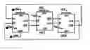
FIG. 3 is a block diagram of a three-stage ring oscillator using delay cells in accordance with the invention;
FIG. 4 shows the calculated and simulated tuning characteristic for a 2400 MHz ring oscillator;
FIG. 5 shows the sensitivity in the frequency of oscillation due to changes in supply voltage for the three-stage ring oscillator; and
FIG. 6 shows the Figure of Merit characteristics for ring oscillators in accordance with the invention compared to the prior art.
DETAILED DESCRIPTION OF THE PREFERRED EMBODIMENTSThe novel delay cell in accordance with the principles of the invention employs a resistive element, such as a resistor, as a common source for a differential amplifier. By using a resistive element instead of a common current source, the performance of the oscillator can be considerably improved.
The delay cell shown in FIG. 1a comprises a differential amplifier 10 consisting of a pair of n-channel MOSFETs M1 and M2 having their substrates connected to ground. The gates of the MOSFETs M1 and M2 are connected to voltage inputs Vin and Vout.
The sources of the MOSFETs M1 and M2 are connected to ground through a common source resistor RSS. The drains are connected through respective load resistors RD to VDD. FIG. 2a shows an equivalent circuit for the MOSFETs.
A varactor arrangement of fingers 12 is connected between the drains of the MOSFETs M1 and M2. The varactor arrangement consists of a pair of p-channel MOSFETs P1 and P2 connected at their gates. The common gate connection provides the control input, Vctrl. The substrates are connected to the drains, and the source of each p-channel MOSFET is connected to its drain. FIG. 2b shows an equivalent circuit for the varactors.
The p-channel MOSFETs have a channel length of 0.18 _82 m and a width of 2.5 μm. They operate in both the depletion and accumulation regions. The differential pair of n-channel MOSFET transistors have a channel length of 0.18 μm and a width of 2.5 μm×4.
The delay cell shown in FIG. 1a was used to design three-, five-, and seven-stage ring oscillators with center frequencies of 1800 MHz, 1900 MHz, and 2400 MHz respectively. The delay cell shown in FIG. 1b was used to design three-, five-, and seven-stage ring oscillators with center frequencies of 450 MHz, 700 MHz, and 900 MHz respectively as well as three-stage ring oscillators with center frequencies of 1800 MHz, 1900 MHz, and 2400 MHz.
In order to understand the operation of the delay cell in accordance with the invention, it is helpful to consider a simple model. The varactors are represented with a lumping equivalent varactor resistance and a lumped variable varactor capacitance. The n-channel MOSFETs are represented by an ideal transistor surrounded by its gate and diffusion capacitance. Although it is known that the delay stage is used to design a voltage-controlled oscillator and that large signals are expected, the ideal transistor is treated assuming small signals.
If the common-mode signals are neglected, then the simplified transfer function in the frequency domain for one stage is given by H ( j ω ) = - G m R D · 1 + j ω C var R var ( 1 - b 2 ω 2 ) + b 1 j ω where ( 1 ) b 1 = C var R var + R D ( C var + C eqv ) ( 2 ) b 2 = R D R var C var C eqv ( 3 ) C eqv = C 1 + C 2 + C BD + C GB + C GS ( 4 ) C 1 = C GD ( 1 + 1 2 G m R D ) ( 5 ) C 2 = C GD ( 1 + 2 G m R D ) . ( 6 )
FIG. 3 shows a three-stage voltage-controlled ring oscillator made up of delay cells of the type shown in FIG. 1a. The cells 30 are connected in a tandem feedback arrangement. The loop gain for this system is,
βA=H(jω))·H(jω)·H(jω)). (7)
Following the Barkhausen criteria, each stage should contribute 60° phase shift in order the oscillation to start, ∠ ( H ( j ω ) ) = π 3 radians . ( 8 )
In the case of the ring oscillator configured with N-stages, each stage should contribute
∠
(
H
(
j
ω
)
)
π
N
radians
(
9
)
phase shift in order for the feedback system to oscillate. Equations (1) and (9) together give
-
τ
2
·
ω
3
+
B
2
tan
(
π
N
)
·
ω
2
+
B
1
·
ω
-
tan
(
π
N
)
=
0
(
10
)
where τvar=CvarRvar, B2=b2+b1·τvar, τ2=b2·τvar, and B1=b1+τvar. The approximated frequency of oscillation for the ring oscillator with N-stages can be calculated from,
f
osc
=
-
B
1
+
B
1
2
+
4
B
2
(
tan
π
N
)
2
2
π
B
2
tan
π
N
.
(
11
)
The equation (11) gives the frequency of oscillation for the feedback system with N-stages. In deriving this expression, the parasitic capacitances due to the layout, such as the overlap capacitances between the metal layers, fringing capacitances, and overlap capacitances between the metal layers and the substrate were ignored. In addition, a source-follower buffer with an n-channel MOSFET with 2.5 μm×5 in width and 0.18 μm in length and one resistor with 444˜ was used. In an ideal situation, the buffer should not load the VCO output. However, in reality the buffer input impedance will load the VCO. It can be shown that the input impedance of the buffer can be assumed as pure capacitive. To simplify the analysis, this capacitance is assumed as parasitic capacitance as well.
The parasitic capacitances were assumed to be distributed throughout the circuit and appear in parallel to the capacitances used in analysis. That means that the value of the capacitors already incorporated during the analysis are increased by the value of the parasitic capacitances. Although each capacitor will see different parasitic capacitance due to the layout, for simplification it can be assumed that each capacitance see additional an average parasitic capacitance Cpar. Hence, if the value of the varactor capacitance Cvar is replaced by Cvar+Cpar, as well as the value of Ceqv is replaced by Ceqv+5●Cpar then the derived formula (11) is more accurate and closer to reality.
FIG. 4 shows the calculated and simulated tuning characteristic of the 2400 MHz ring oscillator with three stages and varactor with one finger. From the simulated results was found that the average value of the parasitic capacitances is approximately Cpar=2.75[fF ]. The maximum deviation between the simulated and calculated curve is 1%.
Table 1 shows the calculated sensitivity of the frequency of oscillation due to ±50% variations of the MOSFET parameters.
| TABLE I | ||||||
| ±50[%] | CBD | CGB | CGD | CGS | Gm | |
| fosc[%] | ±5.0 | ±2.3 | ±17.4 | ±8.0 | ±5.2 | |
The effect of the MOSFET parameters on the estimated frequency of oscillation a three-stage ring oscillator with center frequency at 900 [MHz] was considered.
If the nominal value of the frequency of oscillation is assumed when Vctr1=0.9[V ] then Table I shows the sensitivity of the derived formula (11) if some of the parameters such as CBD, CGB, CGD, CGS, and Gm change the value by ±50%. The idea is to show that the ±50% does not result in abrupt changes of the estimated oscillation frequency. Note that the actual deviation is expected to be less than 50%. The 50% error was taken as an extreme. According to the Table I, the gate-to-drain CGD capacitance is the most critical parameter in estimating the frequency of oscillation.
Table II shows how the frequency of oscillation for some measured ring oscillators is affected due to process tolerance of the resistor RDD.
| TABLE II | ||||
| RDD | fosc(RDD) | |||
| RO | N | Varactor | [%] | [%] |
| 1800 | 3 | ×1 | −24.4 | 32.2 |
| 1900 | 3 | ×1 | −21.9 | 28.0 |
| 2400 | 3 | ×1 | −12.6 | 14.4 |
| 1800 | 5 | ×1 | +7.4 | −6.9 |
| 1900 | 5 | ×1 | +17.4 | −14.8 |
| 2400 | 5 | ×1 | +24.1 | −19.4 |
| 1800 | 7 | ×1 | +34.3 | −25.5 |
| 1900 | 7 | ×1 | +34.5 | −25.6 |
| 2400 | 7 | ×1 | +27.6 | −21.5 |
FIG. 5 shows how the frequency of oscillation, of the three-stage 2400 [MHz] ring oscillator, is sensitive to the supply voltage.
In the event the simulation tool does not take into account all capacitances associated with the oscillator's layout, then the fabricated oscillator will have “an extra” parasitic capacitance. If extra parasitic capacitance appears on the VCO loop, the value of Cvar and Ceqv will be increased. Table III shows the estimated values of Cextra and affect on the frequency of oscillation. Note that the effect of the extra capacitance can be minimized by increasing the number of stages.
It can be shown that for the N-stage ring oscillator presented in this paper the phase noise is given by It can be shown that for the N-stage ring oscillator presented in this paper the phase noise is given by
PN
=
2
N
i
N
2
V
pp
2
(
1
+
(
tan
180
°
N
)
2
)
·
R
2
Q
2
(
ω
osc
Δ
ω
)
2
(
12
)
where, if Gm is known, the resistor R can be calculated from:
G
m
R
=
1
+
(
tan
(
180
°
N
)
)
2
.
(
13
)
The open-loop quality factor, Q, of the system is
Q
=
N
2
·
tan
180
°
N
1
+
(
tan
180
N
)
2
.
(
14
)
The thermal noise current per unit bandwidth is
i
N
2
_
=
4
kT
(
γ
I
SS
E
C
L
eff
+
1
R
D
+
1
R
var
)
.
(
15
)
where the coefficient γ has value between 1 and 2 for short-channel devices [1], EC≈4×10⁶[v/m] is the critical electric field in the silicon [1] , and Rvar is the parallel resistance of the varactor.
Table IV shows the calculated, simulated and measured phase noise for some of the ring oscillators presented with this paper. Note that the flicker noise was ignored by the calculated results. The measured results were obtained by single-ended measurements.
| TABLE IV | ||||
| RO [MHz] | Varactor | calculated | simulated | measured |
| 1800 | ×3 | −99.5d | −96.3d | −95.1s |
| 1800 | ×1 | −97.8d | −96.8d | −95.2s |
| 1900 | ×3 | −99.0d | −95.9d | −92.6s |
| 1900 | ×1 | −98.0d | −97.3d | −93.6s |
| 2400 | ×3 | −99.8d | −94.1d | −91.6s |
| 2400 | ×1 | −97.0d | −96.1d | −93.1s |
The stimulated tuning curve for ring oscillators incorporating the novel delay cells can be simulated with a second-order polynomial of the form:
Fosc=a2x2+a1x+a0
where x is the control signal.
FIG. 6 gives a comparison of the Figure of Merit (FOM) of the ring oscillators in accordance with embodiments of the invention and the prior art. The FOM was determined using the equation FOM = PN ( ω 0 , Δω ) - 10 log ( [ mW ] P VCO ( ω 0 Δω ) 2 ) ( 20 )
Table V shows the summarized results for the ring oscillators in accordance with the invention. The same table includes the calculated values for cycle-to-cylce jitter assuming a white noise in the oscillator, Δ T cc 2 ≈ 4 π ω o 3 S ϕ ( ω ) ( ω - ω o ) 2 ( 21 )
where Sφ(ω) is the phase noise with the respect to the carrier, ωo is the oscillation frequency, and (ω-ωo) is the offset frequency.
| TABLE V | |||||||||||
| core | |||||||||||
| Supply | Itail | P | f | Kvco | PN | offset | FOM | area | jitter | ||
| N | [V] | [mA] | [mW] | [MHz] | [MHz/V] | [dBc/Hz] | [MHz] | [dB] | [μm2] | [ps] | Design |
| 3 | 1.8 | 0.088 | 0.474 | 457a | 30.5 | −106.3 | 1.0 | −162.5 | 3602 | 1.81 | Invention |
| 5 | 1.8 | 0.153 | 1.377 | 453a | 35.5 | −111.9 | 1.0 | −163.6 | 5440 | 0.94 | Invention |
| 7 | 1.8 | 0.244 | 3.069 | 457a | 30.4 | −114.6 | 1.0 | −162.9 | 6623 | 0.68 | Invention |
| 3 | 1.8 | 0.129 | 0.699 | 703a | 48.5 | −104.7 | 1.0 | −163.1 | 3144 | 1.11 | Invention |
| 5 | 1.8 | 0.258 | 2.319 | 703a | 48.0 | −109.7 | 1.0 | −163.0 | 4717 | 0.63 | Invention |
| 7 | 1.8 | 0.390 | 4.914 | 703a | 43.7 | −112.6 | 1.0 | −162.6 | 5840 | 0.45 | Invention |
| 3 | 1.8 | 0.172 | 0.931 | 903a | 57.0 | −103.1 | 1.0 | −162.5 | 2812 | 0.91 | Invention |
| 5 | 1.8 | 0.346 | 3.112 | 903a | 56.4 | −108.4 | 1.0 | −162.6 | 4717 | 0.50 | Invention |
| 7 | 1.8 | 0.510 | 6.428 | 903a | 51.2 | −111.3 | 1.0 | −162.3 | 5840 | 0.36 | Invention |
| 3 | 1.8 | 0.331 | 1.787 | 1836a | 113.7 | −96.3 | 1.0 | −159.1 | 2480 | 0.69 | Invention |
| 3 | 1.8 | 0.283 | 1.529 | 1800b | 50.8 | −96.8 | 1.0 | −160.0 | 4234 | 0.67 | Invention |
| 5 | 1.8 | 0.697 | 6.275 | 1804b | 47.6 | −101.2 | 1.0 | −158.4 | 7123 | 0.40 | Invention |
| 7 | 1.8 | 1.235 | 15.567 | 1802b | 40.5 | −105.0 | 1.0 | −158.2 | 9526 | 0.26 | Invention |
| 3 | 1.8 | 0.344 | 1.875 | 1925a | 124.5 | −95.9 | 1.0 | −158.9 | 2480 | 0.67 | Invention |
| 3 | 1.8 | 0.311 | 1.681 | 1902b | 53.4 | −97.3 | 1.0 | −160.6 | 4234 | 0.58 | Invention |
| 5 | 1.8 | 0.762 | 6.855 | 1899b | 49.0 | −101.3 | 1.0 | −158.5 | 7123 | 0.37 | Invention |
| 7 | 1.8 | 1.314 | 16.562 | 1900b | 40.8 | −104.7 | 1.0 | −158.0 | 9555 | 0.25 | Invention |
| 3 | 1.8 | 0.413 | 2.228 | 2430a | 129.2 | −94.1 | 1.0 | −158.3 | 2480 | 0.58 | Invention |
| 3 | 1.8 | 0.414 | 2.234 | 2399b | 66.6 | −96.1 | 1.0 | −160.2 | 4234 | 0.47 | Invention |
| 5 | 1.8 | 1.049 | 9.444 | 2402b | 64.3 | −100.4 | 1.0 | −158.2 | 7123 | 0.29 | Invention |
| 7 | 1.8 | 1.702 | 21.443 | 2401b | 47.5 | −103.0 | 1.0 | −157.3 | 9902 | 0.21 | Invention |
| 12 | 2.5 | 0.33 | 10.0 | 447 | n/a | −109.5 | 1.0 | −152.5 | n/a | 1.26 | Prior art |
| 8 | 2.5 | 0.50 | 10.0 | 731 | n/a | −106.2 | 1.0 | −153.5 | n/a | 0.88 | Prior art |
| 2 | 2.5 | 3.13 | 15.4 | 900 | 630 | −105.5 | 0.6 | −157.2 | 12750 | 0.42 | Prior art |
| 3 | 1.8 | 3.56 | 19.2 | 900 | 656 | −109.0 | 0.6 | −159.7 | 6750 | 0.28 | Prior art |
| 2 | 3.3 | 12.0 | 79.2 | 973 | n/a | −117.0 | 1.0 | −157.1 | n/a | 0.16 | Prior art |
| 3 | 3.3 | 0.30 | 3.0 | 1250 | 145 | −100.0 | 1.0 | −157.2 | n/a | 0.80 | Prior art |
| 4 | 3.0 | 2.50 | 30.0 | 900 | 300 | −117.0 | 0.6 | −165.8 | 99200 | 0.11 | Prior art |
aMOS varactor with three fingers |
|||||||||||
bMOS varactor with one finger |
|||||||||||
Vctrl = 1.0[V] |
Improvements of the phase noise and cycle-to-cycle jitter can be accomplished by increasing the number of delay stages. Increasing the number of stages from three to five, or five to seven, or seven to nine, improved the phase noise by 4-5 dBc/Hz. By increasing the number of stages the voltage swing of the VCO output signal can increased, the delay of the stages reduced, and the switching speed increased. These effects directly improve the phase.
The ring oscillators using the delay cells of this invention can be fabricated using 0.18 μm CMOS technology. The ring oscillators have a lower power dissipation, an FOM comparable with CMOS oscillators, and a small core layout area.
Claims
We claim:1. A delay cell for use in a voltage controlled oscillator comprising:
a differential amplifier having a pair of outputs;
a common resistive element supplying current to said differential amplifier;
a varactor arrangement between said outputs having a control input; and
a pair of load resistive elements connected to said respective pair of outputs.
2. The delay cell of claim 1, comprising a plurality of said varactor arrangements connected between said respective outputs, said varactor arrangements having a common control input.
3. The delay cell of claim 1, wherein each varactor arrangement comprises a pair of back-to-back MOSFETs connected at their respective gates.
4. The delay cell of claim 3, wherein said MOSFETs are configured to operate in both the depletion and accumulation regions.
5. The delay cell of claim 4, wherein said MOSFETs are p-channel MOSFETs.
6. The delay cell of claim 5, wherein said p-channel MOSFETs have a channel length of about 0.18 μm and a width of about 2.5 μm.
7. The delay cell of claim 5, wherein said differential amplifier comprises a pair of MOSFETs arranged in a differential configuration.
8. The delay cell of claim 7, wherein said MOSFETs forming said differential amplifier are n-channel MOSFETs.
9. The delay cell of claim 1, wherein said load resistive elements are resistors.
10. The delay cell of claim 6, wherein said common resistive element supplying current is a common source resistor.
11. The delay cell of claim 10, wherein said common source resistor is directly connected between the source of each of said MOSFETs forming said differential amplifier and ground.
12. A voltage controlled oscillator comprising a plurality of cascaded delay cells connected as a ring oscillator, each delay cell comprising:
a differential amplifier having a pair of outputs;
a common resistive element supplying current to said differential amplifier;
a varactor arrangement between said outputs having a control input; and
a pair of load resistive elements connected to said respective outputs.
13. The voltage controlled oscillator claim 12, wherein each delay cell comprises a plurality of varactor arrangements connected between said respective outputs, said varactor arrangements having a common control input.
14. The voltage controlled oscillator of claim 13, wherein each varactor arrangement comprises a pair of back-to-back MOSFETs connected at their respective gates.
15. The voltage controlled oscillator of claim 14, wherein said MOSFETs are configured to operate in both the depletion and accumulation regions.
16. The voltage controlled oscillator of claim 15, wherein said MOSFETs are p-channel MOSFETs.
17. The voltage controlled oscillator of claim 12, wherein said differential amplifier comprises a pair of n-channel MOSFETs arranged in a differential configuration, and said common resistive element supplying current is a common source resistor.
18. A method of determining the frequency of oscillation of ring oscillator comprising N delay stages, each delay stage including a differential amplifier having a pair of outputs; a common source resistive element supplying current to said differential amplifier; a varactor arrangement between said outputs having a control input; and a pair of load resistive elements connected to said respective outputs, said method comprising computing the frequency of oscillation by evaluating the expression:
f osc = - B 1 + B 1 2 + 4 B 2 ( tan π N ) 2 2 π B 2 tan π N
where B1 and B2 depend on the circuit parameters defined herein.
Images & Drawings included:


Sources:
- United States Patent and Trademark Office - verify current appl. status at the USPTO↗
Recent applications in this class:
- » 20250260393 2025-08-14
INJECTION LOCKED PHASE ROTATOR - » 20240396533 2024-11-28
OSCILLATION RING CIRCUIT AND APPARATUS AND METHOD FOR MEASURING READING TIME OF SEQUENTIAL CIRCUIT - » 20240223165 2024-07-04
Oscillation device and method for oscillation thereof - » 20230396240 2023-12-07
THREE-STAGE DIFFERENTIAL RING OSCILLATOR GENERATING DIFFERENTIAL IN-PHASE AND QUADRATURE-PHASE CLOCKS - » 20230179185 2023-06-08
Glitch-free frequency tuning of ring-oscillators - » 20230179184 2023-06-08
Delay cell circuits - » 20220376683 2022-11-24
Voltage controlled oscillator and control method thereof, P2P interface circuit, electronic device - » 20220294432 2022-09-15
Multiple adjacent slicewise layout of voltage-controlled oscillator - » 20210281249 2021-09-09
Multiple adjacent slicewise layout of voltage-controlled oscillator - » 20210036691 2021-02-04
Ring oscillator and method for controlling start-up of ring oscillator