Housing of circuit boards
US20070020971A1
2007-01-25
11/479,474
2006-06-30
✅ Patent granted
US 7,293,999 B2
2007-11-13
-
-
Gary Paumen
2026-06-30
Abstract:
A fibre optic module has a PCB with high frequency tracks. The PCB is housed within a housing having top and bottom parts, each having a series of metallized ridges. The PBC has through holes filled with solder. Thus, there is a series of electrical interconnections through the PBC, and the total length of any enclosed periphery is much shorter than the full periphery of the board so that high frequencies are attenuated.
Inventors:
- Keith Everett 1 🇬🇧 Edmunds, United Kingdom
- Kevin Paul Little 1 🇬🇧 Barham, United Kingdom
- Jamie Anderson 1 🇬🇧 Ipswich, United Kingdom
- Keith Everett 1 🇬🇧 Suffolk, United Kingdom
- Kevin Paul Little 1 🇬🇧 Suffolk, United Kingdom
- Jamie Anderson 1 🇬🇧 Suffolk, United Kingdom
Assignee:
- Avago Technologies General IP (Singapore) Pte. Ltd. 1,894 🇸🇬 Singapore, Singapore
Interested in similar patents?
Get notified when new applications in this technology area are published.
Classification:
H05K1/0218 » CPC main
Printed circuits; Details; Electrical arrangements not otherwise provided for; Reduction of cross-talk, noise or electromagnetic interference by printed shielding conductors, ground planes or power plane
H05K1/0218 » CPC main
Printed circuits; Details; Electrical arrangements not otherwise provided for; Reduction of cross-talk, noise or electromagnetic interference by printed shielding conductors, ground planes or power plane
H05K9/0058 » CPC further
Screening of apparatus or components against electric or magnetic fields; Casings specially adapted for optoelectronic applications
H05K9/0058 » CPC further
Screening of apparatus or components against electric or magnetic fields; Casings specially adapted for optoelectronic applications
H05K3/325 » CPC further
Apparatus or processes for manufacturing printed circuits; Assembling printed circuits with electric components, e.g. with resistor electrically connecting electric components or wires to printed circuits by abutting or pinching, i.e. without alloying process; mechanical auxiliary parts therefor
H05K2201/09481 » CPC further
Indexing scheme relating to printed circuits covered by; Shape and layout; Shape and layout details of conductors; Pads and lands Via in pad; Pad over filled via
H05K2201/09481 » CPC further
Indexing scheme relating to printed circuits covered by; Shape and layout; Shape and layout details of conductors; Pads and lands Via in pad; Pad over filled via
H05K2201/09572 » CPC further
Indexing scheme relating to printed circuits covered by; Shape and layout; Shape and layout details of conductors; Conductive through-holes or vias Solder filled plated through-hole in the final product
H05K2201/09572 » CPC further
Indexing scheme relating to printed circuits covered by; Shape and layout; Shape and layout details of conductors; Conductive through-holes or vias Solder filled plated through-hole in the final product
H05K2201/09972 » CPC further
Indexing scheme relating to printed circuits covered by; Shape and layout; Shape or layout details not covered by a single group of - Partitioned, e.g. portions of a PCB dedicated to different functions; Boundary lines therefore; Portions of a PCB being processed separately or differently
H05K2201/10371 » CPC further
Indexing scheme relating to printed circuits covered by; Details of components or other objects attached to or integrated in a printed circuit board; Other objects, e.g. metallic pieces Shields or metal cases
H05K2201/10371 » CPC further
Indexing scheme relating to printed circuits covered by; Details of components or other objects attached to or integrated in a printed circuit board; Other objects, e.g. metallic pieces Shields or metal cases
H05K1/00 IPC
Printed circuits
H05K1/00 IPC
Printed circuits
H01R12/00 IPC
Structural associations of a plurality of mutually-insulated electrical connecting elements, specially adapted for printed circuits, e.g. printed circuit boards [PCBs], flat or ribbon cables, or like generally planar structures, e.g. terminal strips, terminal blocks; Coupling devices specially adapted for printed circuits, flat or ribbon cables, or like generally planar structures; Terminals specially adapted for contact with, or insertion into, printed circuits, flat or ribbon cables, or like generally planar structures
Description
INTRODUCTIONThe invention relates to support of circuit boards in a housing, particularly circuit boards having high-frequency tracks.
In devices such as fibre optic transceiver modules there are circuit boards having high frequency tracks. For avoidance of damage to such tracks there is typically a gap or space above and below the board, the board being supported on ledges on opposed sides. While this configuration of housing is effective at reducing risk of physical damage, these spaces unfortunately provide a path for high frequency signals and render the module susceptible to interference. This arises particularly if there is a relatively long periphery around the board.
The invention addresses this problem.
STATEMENTS OF INVENTIONAccording to the invention, there is provided an electronic device comprising a circuit board having high frequency tracks and a housing surrounding the board, wherein the housing and the board comprise interconnect means for forming connections between opposed parts of the housing through the board.
In one embodiment, the interconnect means comprises conductors extending through the board for contact with the housing on opposed sides of the board.
In another embodiment, the conductors comprise solder filled into board through-holes.
In a further embodiment, the conductors extend above the surface of the board on at least one side.
In one embodiment, the conductors form bumps on both opposed surfaces of the board.
In another embodiment, the housing comprises protruding features to make electrical connections with the conductors.
In a further embodiment, the protruding features are ridge-shaped.
In one embodiment, the board comprises through-holes and the housing comprises teeth extending through the through holes.
In another embodiment, opposed teeth extend partially through the through-holes to make contact.
In a further embodiment, the opposed teeth extend partially through the board.
In one embodiment, the interconnect means comprises a conductive and resilient connector.
In another embodiment, said connector is in the form of a gasket surrounding the board.
DETAILED DESCRIPTION OF THE INVENTIONThe invention will be more clearly understood from the following description of some embodiments thereof, given by way of example only with reference to the accompanying drawings in which:
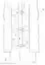
FIG. 1 is a diagrammatic cross-sectional sketch showing a housing and PCB assembly of the invention;
FIG. 2 is a perspective view from above of the assembly with a top housing part removed.
FIG. 3 is a perspective view showing an end of the housing without the board;
FIGS. 4 and 5 are perspective views from above of alternative housing bottom parts;
FIG. 6 is a perspective view showing the end of an alternative assembly, and FIG. 7 shows a bottom housing part in more detail; and
FIG. 8 shows a board and part of a housing of an alternative embodiment.
Referring to FIG. 1 an opto-electronic device 1 comprises a top housing part 10, a bottom housing part 11, and a PCB 2. The PCB 2 has solder 3 filled into through-holes, providing a bump on each side. The housing parts 10 and 11 have ridges 12 and 13 respectively located to engage the protruding solder bumps of the solder 3. The ridges 12 and 13 are metallized with black electroless nickel so that there is a full electrical connection between the parts 10 and 11 through the solder 3. Also, the solder 3 is isolated from the PCB tracks 15, ensuring that there is no adverse impact on -the operation of the PCB's circuit. This is shown clearly in FIG. 2. The configuration of the ridges 12 and 13 is shown more clearly in FIG. 3, triangular in cross-section and being long enough along the apex to ensure good contact with the bump.
Because of the several top-to-bottom interconnections, the total length of any enclosed periphery is much shorter than heretofore. This significantly attenuates high frequencies.
An alternative housing bottom part 21 is shown in FIG. 4. This has a stepped configuration, with ridges 23 on an upper tier.
A housing bottom part 25 having a simpler configuration is shown in FIG. 5. In this embodiment ridges 26 are located along a side edge.
Referring to FIGS. 6 and 7 housing top and bottom parts 30 and 31 have metallised teeth 32 and 33 respectively which extend through apertures in the PCB to directly make physical and electrical contact. As the teeth 32 and 33 make contact there is no need for the apertures in the PCB to be filled or even plated.
Referring to FIG. 8, in another embodiment the housing comprises a conductive EMC gasket 40 through which a PCB 41 is inserted. Only the gasket 40 is illustrated The PCB 41 has filled through-holes 42 for contact with the gasket 40. In this embodiment the gasket has a flat profile, however, it may be toothed.
The conductive elastomer fills the gap around the PCB and hence reduces the peripheral distance, and at the same time provides a cushion for the PCB to prevent mechanical damage. This, together with the through holes in the board provide the short peripheral distances.
Another advantage is that the elasticity of the seal means that there is some mechanical compliance in the arrangement to allow for some mechanical tolerance and to compensate for dimensional changes due to temperature changes.
The invention is not limited to the embodiments described but may be varied in construction and detail.
Claims
1. An electronic device comprising a circuit board having high frequency tracks and a housing surrounding the board, wherein the housing and the board comprise interconnect means for forming connections between opposed parts of the housing through the board.
2. An electronic device as claimed in claim 1, wherein the interconnect means comprises conductors extending through the board for contact with the housing on opposed sides of the board.
3. An electronic device as claimed in claim 2, wherein the conductors comprise solder filled into board through-holes.
4. An electronic device as claimed in claims 2, wherein the conductors extend above the surface of the board on at least one side.
5. An electronic device as claimed in claim 4, wherein the conductors form bumps on both opposed surfaces of the board.
6. An electronic device as claimed in claim 2, wherein the housing comprises protruding features to make electrical connections with the conductors.
7. An electronic device as claimed in claim 6, wherein the protruding features are ridge-shaped.
8. An electronic device as claimed in claim 1, wherein the board comprises through-holes and the housing comprises teeth extending through the through holes.
9. An electronic device as claimed in claim 8, wherein opposed teeth extend partially through the through-holes to make contact.
10. An electronic device as claimed in claim 9, wherein the opposed teeth extend partially through the board.
11. An electronic device as claimed in claim 1, wherein the interconnect means comprises a conductive and resilient connector.
12. An electronic device as claimed in claim 11, wherein said connector is in the form of a gasket surrounding the board.
13-17. (canceled)
Images & Drawings included:


Sources:
- United States Patent and Trademark Office - verify current appl. status at the USPTO↗
Similar patent applications:
- » 11585555
Circuit board housing and circuit board assembly - » 20240049416
CONNECTOR FOR CONNECTING A LINE TO A PRINTED CIRCUIT BOARD, HOUSING HAVING SUCH A CONNECTOR, AND ASSEMBLY COMPRISING A PRINTED CIRCUIT BOARD AND SUCH A HOUSING - » 20090151516
Disassembling tool and method for disassembling a circuit board from a housing, and assembly of a circuit board, a housing and the disassembling tool - » 20170086324
SYSTEM AND METHOD FOR HOUSING CIRCUIT BOARDS OF DIFFERENT PHYSICAL DIMENSIONS - » 20150009639
SYSTEM AND METHOD FOR HOUSING CIRCUIT BOARDS OF DIFFERENT PHYSICAL DIMENSIONS - » 10446462
Printed circuit board housing clamp - » 20120051014
PRINTED CIRCUIT BOARD HOUSING WITH TAPERED LOCKING RAILS - » 20070087592
Two circuit board housing integrated interconnect - » 20140049925
CIRCUIT BOARD HOUSING ASSEMBLY HAVING A SECURING CLIP - » 20170063323
Circuit Board, Housing of Electrical Component and Filter
Recent applications in this class:
- » 20250294668 2025-09-18
Harness PCB - » 20250247947 2025-07-31
ELECTRONIC DEVICE - » 20250240872 2025-07-24
CIRCUIT BOARD AND DISPLAY APPARATUS - » 20250159793 2025-05-15
ELECTRONIC DEVICE - » 20250113429 2025-04-03
OPTICAL MODULE AND FLEXIBLE PRINTED CIRCUIT BOARD - » 20250016910 2025-01-09
SHIELDABLE CIRCUIT BOARD STRUCTURE - » 20250016909 2025-01-09
PRINTED WIRING BOARD - » 20240431019 2024-12-26
Circuit board local electromagnetic shielding - » 20240397608 2024-11-28
FLEXIBLE PRINTED CIRCUIT BOARD AND METHOD FOR MANUFACTURING THE SAME, AND DISPLAY DEVICE - » 20240389219 2024-11-21
MICRO-GROUND VIAS FOR IMPROVED SIGNAL INTEGRITY FOR HIGH-SPEED SERIAL LINKS
Recent applications for this Assignee:
- » 20200066833 2020-02-27
Ultra high density metal-oxide-metal capacitor - » 20200044094 2020-02-06
Semiconductor structure having fin structures with different gate lengths and method of fabricating thereof - » 20200036463 2020-01-30
Leg combining by FFT selection - » 20200014974 2020-01-09
REMOTE CONTROL EXTENDER MECHANISM FOR A SET TOP BOX - » 20190372402 2019-12-05
Multipoint wireless power transfer system and method - » 20190327092 2019-10-24
METHODS AND SYSTEMS FOR SECURE BIOMETRIC AUTHENTICATION - » 20190327019 2019-10-24
Range extension of wireless communication device - » 20190289038 2019-09-19
System for coordinative security across multi-level networks - » 20190278886 2019-09-12
System for secure provisioning and enforcement of system-on-chip (SOC) features - » 20190132743 2019-05-02
Protocols for flexible channel utilization