Surface-mount packaging for chip
US20070114652A1
2007-05-24
11/309,540
2006-08-18
✅ Patent granted
US 7,365,419 B2
2008-04-29
-
-
S. V. Clark
2026-08-18
Abstract:
A chip includes a plurality of pins; and a plurality of symbols defined on a surface of the chip, wherein the symbols are arranged as a graduated scale corresponding with the pins. It becomes very easy to find a initial pin from among the plurality of pins of the chip.
Inventors:
- Ming-Chih HSIEH 130 🇹🇼 Tu-Cheng, Taiwan
- MING-CHIH HSIEH 4 🇹🇼 Tu-Cheng,Taipei Hsien, Taiwan
Assignee:
- HON HAI PRECISION INDUSTRY CO., LTD. 12,833 🇹🇼 Tu-Cheng, Taiwan
- HON HAI PRECISION INDUSTRY CO., LTD. 2,357 🇹🇼 Tu-Cheng, Taipei Hsien, Taiwan
Interested in similar patents?
Get notified when new applications in this technology area are published.
Classification:
H01L23/544 » CPC main
Details of semiconductor or other solid state devices Marks applied to semiconductor devices , e.g. registration marks,
H01L2223/5442 » CPC further
Details relating to semiconductor or other solid state devices covered by the group; Marks applied to semiconductor devices or parts comprising non digital, non alphanumeric information, e.g. symbols
H01L2223/5448 » CPC further
Details relating to semiconductor or other solid state devices covered by the group; Marks applied to semiconductor devices or parts for use after dicing Located on chip prior to dicing and remaining on chip after dicing
H01L2223/54486 » CPC further
Details relating to semiconductor or other solid state devices covered by the group; Marks applied to semiconductor devices or parts for use after dicing Located on package parts, e.g. encapsulation, leads, package substrate
H01L2924/0002 » CPC further
Indexing scheme for arrangements or methods for connecting or disconnecting semiconductor or solid-state bodies as covered by; Technical content checked by a classifier Not covered by any one of groups , and
H01L2924/00 » CPC further
Indexing scheme for arrangements or methods for connecting or disconnecting semiconductor or solid-state bodies as covered by
H01L23/48 IPC
Details of semiconductor or other solid state devices Arrangements for conducting electric current to or from the solid state body in operation, e.g. leads, terminal arrangements ; Selection of materials therefor
Description
FIELD OF THE INVENTIONThe present invention relates to chips, and more particularly to surface-mount packaging for a chip, pins of which are easily identified.
DESCRIPTION OF RELATED ARTUsually, a chip has a lot of pins. Thus, manufacturers should always include some kind of mark or label near the first pin of the chip to facilitate orienting the chip in a correct position for mounting. However, in the design and/or testing process, people often need to count the pins from the first pin to find a specific pin. When the chip has a lot of pins, it will cost much time to find the specific pin and mistakes are easily made.
What is desired, therefore, is a chip, pins of which are easily identified.
SUMMARY OF THE INVENTIONIn one preferred embodiment, a chip includes a plurality of pins, and a plurality of symbols defined on a surface of the chip. The symbols are arranged as a graduated scale corresponding with the pins.
Other advantages and novel features will become more apparent from the following detailed description of preferred embodiments when taken in conjunction with the accompanying drawings, in which:
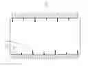
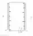
BRIEF DESCRIPTION OF THE DRAWINGSFIG. 1 is a schematic top plan view of a chip, in accordance with a preferred embodiment of the present invention.
DETAILED DESCRIPTION OF THE INVENTIONAs shown in FIG. 1, in a preferred embodiment of the present invention, a chip 100 includes a plurality of pins 10. This embodiment employs a chip having sixty pins as an example. One of the pins 10 is marked as an initial pin 12, for example, employing the first pin of the chip 100 acting as the initial pin 12. A marker 40 is usually made on the chip 100 by chip manufactures to indicate the initial pin 12 for facilitating orienting the chip 100 in a correct position for mounting. A label can also be employed to indicate the initial pin 12.
In a surface of the chip 100, every five of pins 10 is indicated with a first symbol 20 or a second symbol 30. In this embodiment, the first symbol 20 is a short line, and the second symbol 30 is a long line. The first symbol 20 and the second symbol 30 are arranged alternately. For example, the fifth pin counting from the initial pin 12 is signed with the first symbol 20, and the tenth pin counting from the initial pin 12 is signed with the second symbol 20, and so on. That is to say, the first symbols 20 and the second symbols 30 are arranged as a graduated scale corresponding with the pins 10. If a number of one of the pins 10 is a multiple of five but not of ten, the first symbol 20 is assigned thereon. If a number of one of the pins 10 is a multiple of a ten, the second number 30 is signed thereon. The idea can also be expressed as M*Nth pin counting from the initial pin 12 is marked with one of the symbols 20 or the symbols 30, N=1, 2, 3, . . . , n, n is an integer greater than zero, and M is an integer constant. Although in this embodiment, five is used for the increments of the graduated scale other amounts may be selected as desired. Thus, it becomes very easy to identify the initial pin 12 as needed, but other pins as well. Additionally, the first symbols 20 and the second symbols 30 can be markings comprising lines having same length but different colors, or differing symbolic figures, and so on.
It is believed that the present embodiments and their advantages will be understood from the foregoing description, and it will be apparent that various changes may be made thereto without departing from the spirit and scope of the invention or sacrificing all of its material advantages, the examples hereinbefore described merely being preferred or exemplary embodiments.
Claims
What is claimed is:1. A chip comprising:
a plurality of pins; and
a plurality of symbols defined on a surface of the chip, wherein the symbols are arranged as a graduated scale corresponding with the pins.
2. The chip as claimed in claim 1, wherein one of the pins is marked as an initial pin, an M*Nth pin counting from the initial pin is marked with one of the symbols, N=1, 2, 3, . . . , n, n being an integer greater than zero, M is an integer constant.
3. The chip as claimed in claim 2, wherein the M equals five.
4. The chip as claimed in claim 2, wherein one of the symbols marking a 2M*Nth pin counting from the initial pin is different from the other symbols.
5. The heat sink as claimed in claim 4, wherein the one of the symbols marking a 2M*Nth pin is a line longer than the other symbols.
6. A chip comprising:
a body having a pair of opposing side surfaces and a main surface located between the side surfaces;
a plurality of groups of pins extending from the side surfaces;
a plurality of symbols defined in the main surface, each of the symbols corresponding to a group of the pins.
7. The chip as claimed in claim 6, wherein the symbols are arranged as a graduated scale corresponding with the pins.
8. The chip as claimed in claim 7, wherein each group comprises a pair of subgroups, the chip further comprises an additional symbol corresponding each pair of subgroups.
9. The chip as claimed in claim 8, wherein the symbols and the additional symbols are different and alternately arranged on the main surface.
10. The chip as claimed in claim 9, wherein the symbols are longer lines and the additional symbols are shorter lines.
Images & Drawings included:
Sources:
- United States Patent and Trademark Office - verify current appl. status at the USPTO↗
Similar patent applications:
- » 20050269695
Surface-mount chip-scale package
Recent applications in this class:
- » 20250293175 2025-09-18
THREE DIMENSIONAL (3D) MEMORY DEVICE AND FABRICATION METHOD - » 20250285989 2025-09-11
SEMICONDUCTOR DEVICE, ELECTRONIC SYSTEM INCLUDING THE SAME AND METHOD FOR FABRICATING THE SAME - » 20250285988 2025-09-11
DOPED WELL AND ALIGNMENT MARK FOR SEMICONDUCTOR DEVICES - » 20250285987 2025-09-11
ON-THE-FLY ANGULAR ALIGNMENT FOR WRITING 3D FEATURES IN A MOUNTED SUBSTRATE - » 20250279372 2025-09-04
WAFER, WAFER DIE AND METHOD FOR MANUFACTURING WAFER DIE - » 20250279370 2025-09-04
METHOD FOR ALIGNING BACKSIDE PATTERN BASED ON ONE OR MORE FRONTSIDE ALIGNMENT MARKS OF A SEMICONDUCTOR WAFER - » 20250273589 2025-08-28
SEMICONDUCTOR DEVICE INCLUDING MARK STRUCTURE FOR MEASURING OVERLAY ERROR AND METHOD FOR MANUFACTURING THE SAME - » 20250273588 2025-08-28
SEMICONDUCTOR DEVICE AND LASER MARKING METHOD - » 20250273587 2025-08-28
SUBSTRATE FOR ELECTRONIC DEVICE AND METHOD FOR PRODUCING THE SAME - » 20250266369 2025-08-21
UNIQUE DIE PATTERNING FOR DIE ATTACH REFERENCING
Recent applications for this Assignee:
- » 20140233961 2014-08-21
Optical communication module including optical-electrical signal converters and optical signal generators - » 20140083669 2014-03-27
HEAT SINK - » 20140063746 2014-03-06
Electronic device with heat dissipation assembly - » 20140061224 2014-03-06
AUTOMATIC VENDING MACHINE - » 20140060914 2014-03-06
Enclosure with shield apparatus - » 20140058727 2014-02-27
MULTIMEDIA RECORDING SYSTEM AND METHOD - » 20140055955 2014-02-27
Fastener - » 20140055322 2014-02-27
DISPLAY SYSTEM AND HEAD-MOUNTED DISPLAY APPARATUS - » 20140054439 2014-02-27
CONTAINER DATA CENTER WITH SUPPORTING APPARATUS - » 20140054311 2014-02-27
AUTOMATIC VENDING MACHINE WITH MOVING MEMBER FOR PRODUCTS