Semiconductor device with a dummy gate and a method of manufacturing a semiconductor device with a dummy gate
US20070122952A1
2007-05-31
11/563,394
2006-11-27
✅ Patent granted
US 7,528,033 B2
2009-05-05
-
-
Hsien-ming Lee | Kevin Parendo
2026-11-27
Abstract:
A dummy gate may be formed over an isolation layer. A sidewall spacer may be formed next to the dummy gate. The dummy gate and the sidewall spacer may substantially cover or completely cover the edge of isolation layer that is adjacent to an active area of a silicon substrate. Damage to the isolation layer due to a contact hole etching may be prevented, even if there are misalignments.
Assignee:
- Dongbu HiTek Co., Ltd. 896 🇰🇷 Seoul, South Korea
Interested in similar patents?
Get notified when new applications in this technology area are published.
Classification:
H01L21/76232 » CPC main
Processes or apparatus adapted for the manufacture or treatment of semiconductor or solid state devices or of parts thereof; Manufacture or treatment of devices consisting of a plurality of solid state components formed in or on a common substrate or of parts thereof; Manufacture of integrated circuit devices or of parts thereof; Manufacture of specific parts of devices defined in group; Making of isolation regions between components; Dielectric regions, e.g. EPIC dielectric isolation, LOCOS; Trench refilling techniques, SOI technology, use of channel stoppers using trench refilling with dielectric materials of trenches having a shape other than rectangular or V-shape, e.g. rounded corners, oblique or rounded trench walls
Y10S438/926 » CPC further
Semiconductor device manufacturing: process Dummy metallization
H01L29/00 IPC
Semiconductor devices adapted for rectifying, amplifying, oscillating or switching, or capacitors or resistors with at least one potential-jump barrier or surface barrier, e.g. PN junction depletion layer or carrier concentration layer; Details of semiconductor bodies or of electrodes thereof; Multistep manufacturing processes therefor
H01L21/20 IPC
Processes or apparatus adapted for the manufacture or treatment of semiconductor or solid state devices or of parts thereof; Manufacture or treatment of semiconductor devices or of parts thereof the devices having at least one potential-jump barrier or surface barrier, e.g. PN junction, depletion layer or carrier concentration layer the devices having semiconductor bodies comprising elements of Group IV of the Periodic System or AB compounds with or without impurities, e.g. doping materials Deposition of semiconductor materials on a substrate, e.g. epitaxial growth solid phase epitaxy
H01L21/4763 IPC
Processes or apparatus adapted for the manufacture or treatment of semiconductor or solid state devices or of parts thereof; Manufacture or treatment of semiconductor devices or of parts thereof the devices having at least one potential-jump barrier or surface barrier, e.g. PN junction, depletion layer or carrier concentration layer the devices having semiconductor bodies not provided for in groups, , , and with or without impurities, e.g. doping materials; Treatment of semiconductor bodies using processes or apparatus not provided for in groups to change their surface-physical characteristics or shape, e.g. etching, polishing, cutting Deposition of non-insulating, e.g. conductive -, resistive -, layers on insulating layers; After-treatment of these layers
Description
The present application claims priority under 35 U.S.C. 119 and 35 U.S.C. 365 to Korean Patent Application No. 10-2005-0114056 (filed on Nov. 28, 2005), which is hereby incorporated by reference in its entirety.
BACKGROUNDAs some areas of semiconductor manufacturing technology have developed, the degree of integration in semiconductor devices has increased. With increases in the degree of integration, semiconductor manufacturing process margins have decreased. For example, misalignments of a metal interconnection contact during a manufacturing process may create complications.
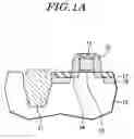
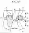
FIGS. 1A to 1C are cross-sectional views which illustrate a structure of a semiconductor device. As illustrated in FIG. 1A, gate oxide layer 12 and gate 13 may be formed over silicon substrate 10. Silicon substrate 10 may have an active area defined by isolation layer 11. An ion implantation process may form a low concentration source/drain 14. Sidewall spacer 15 may be formed by depositing a spacer insulation layer and performing an etching process. An ion implantation process may be implemented, which may use sidewall spacer 15 as a mask, to form a high concentration source/drain 16. Silicide metal may be deposited and heat treated to form silicide layer 17 by a self aligning method.
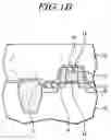
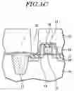
As illustrated in FIG. 1B, etch stop layer 18 maybe deposited. Interlayer dielectric layer 19 may be deposited. As illustrated in FIG. 1C, interlayer dielectric layer 19 may be selectively etched to form contact hole 20. A metal interconnection contact may be formed in contact hole 20 to connect with silicide layer 17 formed over high concentration source/drain 16.
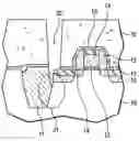
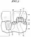
A process of forming a metal interconnection contact in a highly integrated semiconductor device may be susceptible to misalignments. FIG. 2 illustrates an example of a defect that may occur as a result of a misalignment. As illustrated in FIG. 2, contact hole 20 may overlap isolation layer 11 due to a misalignment. Isolation layer 11 may be vulnerable to an etching process employed to etch contact hole 20, which may cause defect 21. Defect 21 may cause junction leakage. Defect 21 may cause an electrical short between a source/drain and a substrate. Defect 21 may degrade characteristics of a semiconductor device. Defect 21 may reduce the yield of semiconductor device manufacturing.
SUMMARYEmbodiments relate to a semiconductor device having a dummy gate. Embodiments relate to a method of manufacturing a semiconductor device having a dummy gate. Embodiments relate to a semiconductor device having a dummy gate selectively formed over an isolation layer, which may prevent defects from forming at an isolation layer. Embodiments may prevent defects from forming, which are the result of a shortage of process margin during a metal interconnection contact manufacturing process in a highly integrated semiconductor device.
Embodiments relate to a semiconductor device and/or a method of manufacturing a semiconductor device with improved process margins when metal interconnection contacts are formed. In embodiments, characteristics of a semiconductor device may be enhanced. In embodiments, manufacturing yield of semiconductor devices may be improved.
In embodiments, a semiconductor device comprises an isolation layer formed over a silicon substrate, which may define an active area on the silicon substrate. A gate oxide layer and a gate may be formed over an active area of a silicon substrate. A dummy gate may be formed over an isolation layer, in accordance with embodiments. A first sidewall spacer may be formed over a gate. A second sidewall spacer may be formed over a dummy gate.
In accordance with embodiments, a semiconductor device may include a dummy gate that may have at least one pattern. A dummy gate and a second sidewall spacer may substantially or completely cover an upper portion of an isolation layer. A second sidewall spacer may substantially or completely cover the edge of an isolation layer adjacent to an active area.
Embodiments relate to a method of manufacturing a semiconductor device, the method may include at least one of the following steps: forming a gate oxide layer and a gate over a silicon substrate on which an active area is defined by an isolation layer and forming a dummy gate over the isolation layer at the same time; and/or simultaneously forming a first sidewall spacer next to a gate and a second sidewall spacer next to a dummy gate by depositing a spacer insulation layer over the entire surface of a silicon substrate and then etching the entire surface of the silicon substrate. In embodiments, a second sidewall spacer may substantially or completely cover the edge of an isolation layer adjacent to an active area.
BRIEF DESCRIPTION OF DRAWINGSFIGS. 1A to 1C are cross-sectional views illustrating a structure of a semiconductor device and a method of manufacturing a semiconductor device.
FIG. 2 is a cross-sectional view illustrating an example defect occurring in a semiconductor device.
Example FIGS. 3A to 3F are cross-sectional views illustrating the structure of a semiconductor device, in accordance with embodiments.
Example FIG. 4 is a cross-sectional view illustrating the structure of a semiconductor device, according to embodiments.
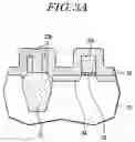
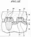
DETAILED DESCRIPTIONExample FIGS. 3A to 3F are cross-sectional views illustrating a structure of a semiconductor device and a method of manufacturing a semiconductor device, according to embodiments. As illustrated in FIG. 3A, gate oxide layer 32 and gate 33a may be formed over silicon substrate 30. Silicon substrate 30 may have an active area defined by isolation layer 31. Dummy gate 33b may be formed over isolation layer 31. Dummy gate 33b may be formed at the same time as gate 33a is formed. The formation of dummy gate 33b and/or gate 33a may be accomplished by changing a mask pattern that forms gate 33a. Dummy gate 33b may not have any electrical function.
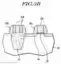
After forming gate 33a and/or dummy gate 33b, ion implantation may be performed to form a low concentration source/drain 34. Spacer insulation layer 35 may be deposited over the entire surface of silicon substrate 30. As illustrated in FIG. 3B, spacer insulation layer 35 may be etched to form sidewall spacer 35a and/or sidewall spacer 35b. First sidewall spacer 35a may be formed next to common gate 33a. Second sidewall spacer 35b may be formed next to dummy gate 33b. Dummy gate 33b and second sidewall spacer 35b may be formed to completely cover or substantially cover the upper portion of isolation layer 31. Second sidewall spacer 35b may be formed to completely cover or substantially cover the edge of isolation layer 31, adjacent to an active area.
As illustrated in FIG. 3C, an ion implantation process may be implemented. An ion implantation process may use first sidewall spacer 35a and second sidewall spacer 35b as a mask. An ion implantation process may form a high concentration source/drain 36 in an active area of silicon substrate 30.
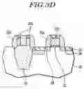
As illustrated in FIG. 3D, silicide metal may be deposited and heat treated to form silicide layer 37, which may be through a self aligning process. Silicide layer 37 may be formed in high concentration source/drain 36, in gate 33a, and/or in dummy gate 33b.
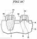
As illustrated in FIG. 3E, etch stop layer 38 maybe deposited. Interlayer dielectric layer 39 may be deposited. As illustrated in FIG. 3F, interlayer dielectric layer 39 may be selectively etched to form contact hole 40. A metal interconnection contact may be formed in contact hole 40 to connect with silicide layer 37.
Even though contact hole 40 and isolation layer 31 may overlap (e.g. due to a misalignment occurring during the process of forming contact hole 40), isolation layer 31 may be undamaged during etching of contact hole 40. Isolation layer 31 may be undamaged because dummy gate 33b and/or second sidewall spacer 35b may be formed over isolation layer 31. Dummy gate 33b may protect isolation layer 31 during formation of a metal interconnection contact. Dummy gate 33b may be selectively formed on only a portion of an isolation layer, according to embodiments, to compensate for process margin. In embodiments illustrated in FIGS. 3A through 3F, two separated dummy gates 33b may be formed over isolation layer 31.
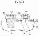
FIG. 4 is a cross-sectional view illustrating a structure of a semiconductor device, according to embodiments. Patterned dummy gate 43b may be formed, according to embodiments. The pattern shape of dummy gate 33b and dummy gate 43b may improve process margin and/or may protect isolation layer 31 during formation of a metal interconnection contact, according to embodiments.
In accordance with embodiments, a dummy gate may be simultaneously formed with a common gate. A second sidewall spacer may be simultaneously formed next to a dummy gate with a first sidewall spacer of a gate. In embodiments, a dummy gate and a second sidewall spacer may completely cover or substantially cover an upper portion of an isolation layer, which may protect the isolation layer. In embodiments, an edge of an isolation layer (e.g. adjacent to an active area) maybe prevented from being damaged during etching of a contact hole, even if some misalignments are present. In embodiments, a process margin of a metal interconnection contact process may be improved. In embodiments, characteristics and/or yield of a semiconductor device may be improved.
A dummy gate may provide no electrical function and may serve to protect an isolation layer during formation of a metal interconnection contact, in accordance with embodiments. In embodiments, a dummy gate may not be formed over every isolation layer and may be selectively formed in areas having insufficient process margin. Additional apparatuses or processes of forming a dummy gate may not be necessary, in some embodiments.
It will be apparent to those skilled in the art that various modifications and variations can be made to embodiments. Thus, it is intended that embodiments cover modifications and variations thereof within the scope of the appended claims.
Claims
What is claimed:1. A semiconductor device comprising:
an isolation layer formed in a silicon substrate; and
a dummy gate formed over the isolation layer.
2. The semiconductor device of claim 1, wherein the isolation layer defines an active area of the silicon substrate.
3. The semiconductor device of claim 1, wherein:
a gate oxide layer and a gate are formed over an active area of the silicon substrate; and
a first sidewall spacer is formed next to the gate.
4. The semiconductor device of claim 1, wherein the dummy gate includes at least one pattern.
5. The semiconductor device of claim 1, wherein a second sidewall spacer is formed next to the dummy gate.
6. The semiconductor device of claim 5, wherein the dummy gate and the second sidewall spacer substantially cover an upper portion of the isolation layer.
7. The semiconductor device of claim 5, wherein the dummy gate and the second sidewall spacer completely cover an upper portion of the isolation layer.
8. The semiconductor device of claim 5, wherein the second sidewall spacer substantially cover an edge of the isolation layer that is adjacent to the active area.
9. The semiconductor device of claim 5, wherein the second sidewall spacer completely cover an edge of the isolation layer that is adjacent to the active area.
10. A method of manufacturing a semiconductor device comprising:
forming a gate over a silicon substrate; and
forming a dummy gate over the silicon substrate.
11. The method of claim 10, wherein the gate and the dummy gate are formed simultaneously.
12. The method of claim 10, comprising forming a gate oxide layer over the silicon substrate.
13. The method of claim 10, comprising forming an isolation layer in the silicon substrate.
14. The method of claim 13, wherein an active area of the silicon substrate is defined by the isolation layer.
15. The method of claim 13, wherein the dummy gate is formed over the isolation layer.
16. The method of claim 10, comprising:
forming a first sidewall spacer next to the gate; and
forming a second sidewall spacer next to the dummy gate.
17. The method of claim 16, wherein the first sidewall spacer and the second sidewall spacer are formed simultaneously.
18. The method of claim 16, wherein the first sidewall spacer and the second sidewall spacer are formed by depositing a spacer insulation layer over an entire surface of the silicon substrate and selectively etching the spacer insulation layer.
19. The method of claim 16, wherein the second sidewall spacer substantially cover an edge of the isolation layer that is adjacent to an active area.
20. The method of claim 19, wherein the second sidewall spacer completely covers an edge of the isolation layer that is adjacent to an active area.
Images & Drawings included:
Sources:
- United States Patent and Trademark Office - verify current appl. status at the USPTO↗
Similar patent applications:
- » 20210057409
Method for manufacturing semiconductor device including dummy gate electrodes - » 20070172997
Method of manufacturing semiconductor device using dummy gate wiring layer - » 9735005
Semiconductor device having dummy gates and its manufacturing method - » 20060038233
C-shaped dummy gate electrode semiconductor device and method of manufacturing the same - » 20190189798
Trench gate semiconductor device with dummy gate electrode and manufacturing method of the same - » 20200343364
Semiconductor device including dummy gate patterns and manufacturing method thereof - » 20240096705
Semiconductor devices including dummy gate dielectric layer and methods of manufacturing thereof - » 20120237879
Pattern forming method, semiconductor device manufacturing method and phase shift photomask having dummy gate patterns - » 20060210889
Pattern forming method, semiconductor device manufacturing method and phase shift photomask having dummy gate patterns - » 20100255423
Pattern forming method, semiconductor device manufacturing method and phase shift photomask having dummy gate patterns
Recent applications in this class:
- » 20250174490 2025-05-29
SEMICONDUCTOR DEVICE AND METHOD OF MANUFACTURING THE SAME - » 20250149376 2025-05-08
HIGH VOLTAGE SEMICONDUCTOR DEVICE INCLUDING ISOLATION REGION - » 20250087530 2025-03-13
LATERAL ETCHING PROCESS TO REMOVE METAL GATE FOOT STRUCTURES - » 20250062158 2025-02-20
SEMICONDUCTOR DEVICE STRUCTURE WITH GATE SPACER AND METHOD FOR FORMING THE SAME - » 20240395600 2024-11-28
SEMICONDUCTOR DEVICES AND METHODS OF MANUFACTURING THEREOF - » 20240395599 2024-11-28
HIGH VOLTAGE SEMICONDUCTOR DEVICE AND METHOD OF MANUFACTURING SAME - » 20240347376 2024-10-17
METHOD OF MANUFACTURING SEMICONDUCTOR STRUCTURE HAVING FINS - » 20240332062 2024-10-03
ETCH PROFILE CONTROL OF ISOLATION TRENCH - » 20240213084 2024-06-27
APPARATUSES INCLUDING SHALLOW TRENCH ISOLATION AND METHODS FOR FORMING SAME - » 20240213083 2024-06-27
SEMICONDUCTOR DEVICE AND MANUFACTURING METHOD THEREOF
Recent applications for this Assignee:
- » 20180069111 2018-03-08
ESD protection SCR device - » 20160372592 2016-12-22
Semiconductor device and radio frequency module formed on high resistivity substrate - » 20160372483 2016-12-22
Passive device and radio frequency module formed on high resistivity substrate - » 20160062547 2016-03-03
Method of scanning touch panel and touch integrated circuit for performing the same - » 20150324031 2015-11-12
Touch Panel - » 20150270308 2015-09-24
CMOS IMAGE SENSOR AND METHOD OF MANUFACTURING THE SAME - » 20150262906 2015-09-17
COF type semiconductor package and method of manufacturing the same - » 20150122623 2015-05-07
Touch panel and method of manufacturing the same - » 20150109235 2015-04-23
Touch screen and touch panel including mutual capacitance type and self-capacitance type pixels, and driving method thereof - » 20150062998 2015-03-05
PROGRAMMABLE MEMORY