Method for fabricating capacitor in semiconductor device
US20070122967A1
2007-05-31
11/478,175
2006-06-28
✅ Patent granted
US 7,825,043 B2
2010-11-02
-
-
Lynne A Gurley | Meiya Li
2026-06-28
Abstract:
A method for fabricating a capacitor in a semiconductor device includes: forming a bottom electrode; forming a ZrxAlyOz dielectric layer on the bottom electrode using an atomic layer deposition (ALD) method, wherein the ZrxAlyOz dielectric layer comprises a zirconium (Zr) component, an aluminum (Al) component and an oxygen (O) component mixed in predetermined mole fractions of x, y and z, respectively; and forming a top electrode on the ZrxAlyOz dielectric layer.
Assignee:
- HYNIX SEMICONDUCTOR INC. 2,053 🇰🇷 Icheon-si, South Korea
- HYNIX SEMICONDUCTOR INC. 1,335 🇰🇷 Kyoungki-do, South Korea
Interested in similar patents?
Get notified when new applications in this technology area are published.
Classification:
H01L21/31 IPC
Processes or apparatus adapted for the manufacture or treatment of semiconductor or solid state devices or of parts thereof; Manufacture or treatment of semiconductor devices or of parts thereof the devices having at least one potential-jump barrier or surface barrier, e.g. PN junction, depletion layer or carrier concentration layer the devices having semiconductor bodies comprising elements of Group IV of the Periodic System or AB compounds with or without impurities, e.g. doping materials; Treatment of semiconductor bodies using processes or apparatus not provided for in groups - to form insulating layers thereon, e.g. for masking or by using photolithographic techniques ; After treatment of these layers; Selection of materials for these layers
C23C16/40 » CPC further
Chemical coating by decomposition of gaseous compounds, without leaving reaction products of surface material in the coating, i.e. chemical vapour deposition [CVD] processes characterised by the deposition of inorganic material, other than metallic material; Deposition of compounds, mixtures or solid solutions, e.g. borides, carbides, nitrides Oxides
H01L28/40 » CPC further
Passive two-terminal components without a potential-jump or surface barrier for integrated circuits; Details thereof; Multistep manufacturing processes therefor Capacitors
H01L21/469 IPC
Processes or apparatus adapted for the manufacture or treatment of semiconductor or solid state devices or of parts thereof; Manufacture or treatment of semiconductor devices or of parts thereof the devices having at least one potential-jump barrier or surface barrier, e.g. PN junction, depletion layer or carrier concentration layer the devices having semiconductor bodies not provided for in groups, , , and with or without impurities, e.g. doping materials; Treatment of semiconductor bodies using processes or apparatus not provided for in groups to change their surface-physical characteristics or shape, e.g. etching, polishing, cutting to form insulating layers thereon, e.g. for masking or by using photolithographic techniques ; After-treatment of these layers
Description
BACKGROUNDThe present invention relates to a method for fabricating a semiconductor device; and more particularly, to a method for fabricating a capacitor in a semiconductor device.
As semiconductor devices such as DRAM become highly integrated, the unit cell size and operating voltage decrease. Thus, the device refresh time is often shortened, and a soft error can frequently occur. To overcome these limitations, capacitors need to be developed to have a capacitance of 25 fF per cell or higher and a reduced leakage current.
Generally, a capacitor formed in a structure of nitride and oxide (NO) using Si3N4 as a dielectric material is disadvantageous in capacitance when it comes to large scale integration. There is not enough area to obtain the required capacitance. Instead of using Si3N4, a capacitor structure that uses a high-K dielectric material (e.g., tantalum oxide (Ta2O5), lanthanum oxide (La2O3) or hafnium oxide (HfO2)) in a single dielectric layer is developed to obtain sufficient capacitance. This particular capacitor structure is called a polysilicon-insulator-polysilicon (SIS) structure.
However, a SIS capacitor structure using an Al2O3 dielectric material may have capacitance limitations in 512M level or higher dynamic random access memories (DRAMs). Thus, many researchers are focused on developing other capacitor structures, such as a metal-insulator-metal (MIM) structure using a titanium nitride (TiN) electrode and an HfO2/Al2O3 or HfO2/Al2O3/HfO2 dielectric structure.
When the aforementioned capacitor structure is used, the expected equivalent oxide thickness (Tox) is about 12 Å. To increase capacitance without reducing oxide thickness, capacitor area can be increased with a 3D electrode structure. In DRAM products with sub-70 nm level metal interconnection technology, obtaining cell capacitance of about 25 fF/cell or higher may result in a complex bottom electrode structure. Accordingly, it may be difficult to obtain the desired capacitance if the area of the bottom electrode structure is not enlarged.
Recently, many studies on MIM capacitor structures have made progress. These MIM capacitor structures use a noble metal, e.g., ruthenium (Ru), as an electrode material and Ta2O5 or HfO2 as a single dielectric material.
However, if the equivalent oxide thickness is decreased to about 12 Å or less along with using the Ru electrode, the MIM capacitor is likely to have a high leakage current; about 1 fA per cell in some instances. Accordingly, it may be difficult to implement this MIM capacitor in DRAM with 512M or higher capacity that uses sub-70 nm level interconnection technology.
SUMMARY OF THE INVENTIONAn embodiment of the present invention relates to a method for fabricating a capacitor in a semiconductor device, where the leakage current is reduced and capacitance increased for DRAM products implemented with sub-70 nm level interconnection technology.
In accordance with an embodiment of the present invention, there is provided a method for fabricating a capacitor in a semiconductor device, including: forming a bottom electrode; forming a ZrxAlyOz dielectric layer on the bottom electrode using an atomic layer deposition (ALD) method, wherein the ZrxAlyOz dielectric layer comprises a zirconium (Zr) component, an aluminum (Al) component and an oxygen (O) component mixed in predetermined mole fractions of x, y and z, respectively; and forming a top electrode on the ZrxAlyOz dielectric layer.
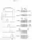
BRIEF DESCRIPTION OF THE DRAWINGSFIG. 1 is a diagram illustrating a capacitor structure in accordance with an embodiment of the present invention;
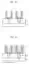
FIGS. 2A to 2C are cross-sectional views illustrating a method for fabricating a capacitor in a semiconductor device in accordance with an embodiment of the present invention; and
FIG. 3 is a diagram for describing sequential operations of forming a ZrxAlyOz dielectric layer based on an atomic layer deposition (ALD) method in accordance with an embodiment of the present invention.
DETAILED DESCRIPTION OF THE INVENTIONSpecific embodiments of the present invention will be described in detail with reference to the accompanying drawings, where like reference numerals denote like elements in different drawings.
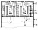
Referring to FIG. 1, a ZrxAlyOz dielectric layer 16 and a top electrode 17 are sequentially formed on a bottom electrode 15. The ZrxAlyOz dielectric layer 16 contains controlled mole fractions of zirconium (Zr), aluminum (Al) and oxygen (O). Also, the ZrxAlyOz dielectric layer 16 is formed using an atomic layer deposition (ALD) method to an approximate thickness between 50 Å and 100 Å.
In the ZrxAlyOz dielectric layer 16, the subscripts x, y and z in “ZrxAlyOz” represent mole fractions of Zr, Al and O, respectively. When added together (i.e., x+y+z) these mole fractions come to approximately 1. Also, the ratio of x to y is in an approximate range between 1:1 and 10:1. This ratio indicates that the mole fraction of the Zr component in the ZrxAlyOz dielectric layer 16 can range from being equal to the Al component to being 10 times greater than the Al component.
Referring to FIG. 2A, an inter-layer insulation layer 12 is formed over a substrate 11 in which bottom structures including bit lines and transistors are already formed. The inter-layer insulation layer 12 is etched to form contact holes 13 exposing the junction regions of the substrate 11 or the landing plug polys (LPPs). A conductive material fills the contact holes 13 to form storage node contacts 14.
A bottom electrode material is formed over the inter-layer insulation layer 14 and the storage node contacts 14. Then a chemical mechanical polishing (CMP) process or an etch-back process is performed on the bottom electrode material to isolate and create each bottom electrode 15 contacting a storage node contact 14.
The bottom electrodes 15 include a metal-based material consisting of either titanium nitride (TiN), tantalum nitride (TaN), tungsten (W), tungsten nitride (WN), ruthenium (Ru), ruthenium oxide (RuO2), iridium (Ir), iridium oxide (IrO2), or platinum (Pt). Also, the bottom electrodes 15 are formed to a thickness ranging from approximately 200 Å to 500 Å. In addition to a cylindrical structure as illustrated in FIG. 2A, the bottom electrodes 15 can be formed in another structure such as a concave structure or a stacked structure.
As an example, if the bottom electrodes 15 use TiN, TiCl4 is used as a source material and NH3 as a reaction gas. The source material and the reaction gas are provided individually at a rate ranging from approximately 10 sccm to 1,000 sccm. At this time, the reaction chamber is maintained at approximately 0.1 Torr to 10 Torr, and the substrate 11 is maintained at approximately 500° C. to 700° C. The bottom electrodes 15 (i.e., the TiN layer) are formed to a thickness ranging from approximately 200 Å to 500 Å.
After the formation of the bottom electrodes 15, an annealing process is performed in an ambient gas selected from the group consisting of nitrogen (N2), hydrogen (H2), N2/H2, oxygen (O2), ozone (O3), and ammonia (NH3). The annealing process is performed to densify the bottom electrodes 15; remove remnant impurities in the bottom electrodes 15, which often cause leakage current to increase; and to eliminate surface roughness, which may cause an uneven electric field distribution.
The annealing process is performed using either a plasma annealing process, a furnace annealing process, or a rapid thermal process (RTP). The plasma annealing process is performed for approximately 1 to 5 minutes under the following conditions: radio frequency (RF) power at approximately 100 W to 500 W to generate a plasma; temperature at approximately 200° C. to 500° C.; pressure at approximately 0.1 Torr to 10 Torr; and the selected ambient gas of approximately 5 sccm to 5,000 sccm. The furnace annealing process is performed at approximately 600° C. to 800° C. using approximately 5 sccm to 5,000 sccm of the selected ambient gas. The RTP is performed using approximately 5 sccm to 5,000 sccm of the selected ambient gas in a chamber maintained in an ascending pressure of approximately 700 Torr to 760 Torr or a descending pressure of approximately 1 Torr to 100 Torr at a temperature of approximately 500° C. to 800° C.
Referring to FIG. 2B, a ZrxAlyOz dielectric layer 16 is formed over the bottom electrodes 15. A thin zirconium oxide (ZrO2) film and a thin aluminum oxide (Al2O3) film are mixed together to form the ZrxAlyOz dielectric layer 16. Particularly, the ZrxAlyOz dielectric layer 16 is obtained by performing an atomic layer deposition (ALD) method, which will be described in detail with reference to FIG. 3.
Referring to FIG. 2C, a top electrode 17 is formed over the ZrxAlyOz dielectric layer 16. The top electrode 17 includes TiN, TaN, W, WN, Ru, RuO2, Ir, IrO2, or Pt. The illustrated capacitor structure is a MIM capacitor structure.
As an example, the top electrode 17 may be a layer of TiN obtained by performing a chemical vapor deposition (CVD) or a physical vapor deposition (PVD). For the CVD method, TiCl4 and NH3 are used as the source material and reaction gas, respectively. The source material and reaction gas are supplied individually at a rate ranging from approximately 10 sccm to 1,000 sccm. At this time, the reaction chamber is maintained at approximately 0.1 Torr to 10 Torr, and the substrate temperature ranges from approximately 500° C. to 600° C. The TiN layer (i.e., the top electrode 17) is formed to a thickness of approximately 200 Å to 400 Å.
Afterwards, an oxide layer or a metal layer may be formed to a thickness of approximately 50 Å to 200 Å. The oxide layer is formed by performing an ALD method and may include a material such as Al2O3, HfO2, Ta2O5, ZrO2, TiO2, or La2O3, and the metal layer may include TiN. The oxide layer or the metal layer is formed as a passivation layer or a buffer layer to improve structural stability against humidity; temperature or electric shocks, which may be generated while a thermal process and a curing process of a subsequent integration process (i.e., a back end process); a wet etching process; a packaging process; and environmental tests for reliability are carried out. For reference, the thermal process and the curing process are performed in an ambient gas such as H2, N2, or N2/H2.
FIG. 3 is a diagram for describing the processes performed in forming a ZrxAlyOz dielectric layer based on an ALD method in accordance with an embodiment of the present invention.
As illustrated, the ALD method includes supplying a source gas, purging out non-reacted parts of the source gas, supplying a reaction gas, and purging out non-reacted parts of the reaction gas. The ALD method is performed repeatedly until the ZrxAlyOz dielectric layer is formed to an intended thickness.
In more detail, the source gas is supplied for adsorption into a target, and the purge gas is supplied to purge out excess source gas that was not adsorbed. Then, the reaction gas is supplied and reacts with the adsorbed source gas to deposit the desired thin layer. The purge gas is then supplied again to purge out non-reacted parts of the reaction gas.
The ZrxAlyOz dielectric layer is obtained by performing the aforementioned unit cycle of the ALD method, including supplying a Zr source gas, an Al source gas, supplying a purge gas, supplying a reaction gas, and supplying the purge gas again. The unit cycle is repeated until the thickness of the ZrxAlyOz dielectric layer ranges from approximately 50 Å to 100 Å. At this point, the substrate is maintained at approximately 200° C. to 500° C., and the reaction chamber is maintained at approximately 0.1 Torr to 1 Torr.
The Zr source gas is selected from ZrCl4, Zr(N(CH3)C2H5)4, Zr(O-tBu)4, Zr(N(CH3)2)4, Zr(N(C2H5)(CH3))4, Zr(N(C2H5)2)4, Zr(TMHD)4, Zr(OiC3H7)3(TMTD), Zr(OtBu)4, or a Zr containing compound. The Zr source gas is supplied into the reaction chamber by a carrier gas, e.g., argon (Ar) gas, which is supplied at a rate ranging from approximately 150 sccm to 250 sccm for approximately 0.1 seconds to 10 seconds.
The purge gas such as N2 or Ar is supplied to purge out non-adsorbed parts of the Zr source gas. The purge gas is supplied at a rate ranging from approximately 200 sccm to 400 sccm for approximately 3 seconds to 10 seconds.
The Al source gas is selected from Al(CH3)3, Al(C2H5)3 or an Al containing compound. The Al source gas is supplied into the reaction chamber with a carrier gas, e.g., Ar gas. The Ar gas is supplied at a rate ranging from approximately 20 sccm to 100 sccm for approximately 0.1 seconds to 5 seconds.
The purge gas, e.g., N2 or Ar gas, is supplied again to purge out non-reacted parts of the Al source gas. The purge gas is supplied at a rate ranging from approximately 200 sccm to 400 sccm for approximately 3 seconds to 10 seconds.
The reaction gas is selected from either O3 (with a concentration of approximately 100 g/m3 to 500 g/m3), O2, O2 plasma, N2O, N2O plasma, or water vapor. The reaction gas reacts with the Zr source gas and the Al source gas to form the ZrxAlyOz dielectric layer. The reaction gas is supplied at a rate ranging from approximately 100 sccm to 1,000 sccm for approximately 3 seconds to 10 seconds.
The purge gas, e.g., N2 gas or Ar gas, is supplied into the chamber to purge out non-reacted parts of the reaction gas remaining inside the chamber. The purge gas is supplied at a rate ranging from approximately 50 sccm to 200 sccm for approximately 3 seconds to 10 seconds.
The above unit cycle of the ALD method is repeatedly performed until the ZrxAlyOz dielectric layer reaches a thickness of approximately 50 Å to 100 Å.
After the ZrxAlyOz dielectric layer is formed, an annealing process is performed in an ambient gas selected from the group consisting of N2, H2, N2/H2, O2, O3, and NH3. The annealing process is performed to densify the ZrxAlyOz dielectric layer; obtain uniformity of the ZrxAlyOz dielectric layer; or to volatize the remaining impurities, which can cause a leakage current. The annealing process is also performed to reduce the surface roughness of other dielectric layers and remove crystallites.
The annealing process involves a plasma annealing process, a furnace annealing process or a RTP. The plasma annealing process is performed for approximately 1 minute to 5 minutes under the following conditions: radio frequency (RF) power at approximately 100 W to 500 W to generate a plasma; temperature at approximately 200° C. to 500° C.; pressure at approximately 0.1 Torr to 10 Torr; and the selected ambient gas at approximately 5 sccm to 5,000 sccm. The furnace annealing process is performed at approximately 600° C. to 800° C. using approximately 5 sccm to 5,000 sccm of the selected ambient gas. The RTP is performed using approximately 5 sccm to 5,000 sccm of the ambient gas in a chamber maintained in an ascending pressure of approximately 700 Torr to 760 Torr or a descending pressure of approximately 1 Torr to 100 Torr at approximately 500° C. to 800° C. The furnace annealing process and the RTP further increases the dielectric constant of the ZrxAlyOz dielectric layer.
According to the embodiments of the present invention, the ZrxAlyOz layer is used as the dielectric material of a capacitor, and this approach achieves required capacitance (e.g., approximately 25 fF per cell) in sub-70 nm level DRAM capacitors; required leakage current (e.g., approximately 0.5 fF per cell or less); and required breakdown voltage (e.g., approximately 2.0 V (at 1 pA per cell) or higher).
Generally, a thin ZrO2 layer has higher band gap energy (Eg) and dielectric constant (ε) than a thin Ta2O5 layer and a thin HfO2 layer. For reference, the thin ZrO2 layer has a band gap energy of approximately 7.8 eV and a dielectric constant (ε) of approximately 20 to 25; the thin Ta2O5 layer has band gap energy of approximately 4.5 eV and a dielectric constant of approximately 25, and the thin HfO2 layer has a band gap energy of approximately 5.7 eV and a dielectric constant of approximately 20. A thin Al2O3 layer, which has a band gap energy of approximately 8.7 eV and a dielectric constant of approximately 9, has better thermal stability than the thin HfO2 layer. Based on these facts, the ZrxAlyOz dielectric layer can improve limitations in leakage current and thermal stability compared with the single dielectric structure of the capacitor, since the ZrxAlyOz dielectric layer has the characteristics of the thin ZrO2 layer and the thin Al2O3 layer.
As a result, the thickness of the equivalent oxide layer of the ZrxAlyOz dielectric layer can be decreased to approximately 12 Å or less. Hence, the capacitor with the ZrxAlyOz dielectric layer can obtain a high capacitance of approximately 30 fF per cell or higher in sub-70 nm DRAM products. Also, as mentioned above, the capacitor according to the embodiments of the present invention can lower leakage current and desired breakdown voltage, thus enabling mass production.
In addition, since the ZrxAlyOz dielectric layer has better thermal stability than the single dielectric layer such as HfO2, electric characteristics are less likely to be degraded during a high thermal process performed in an integration process after the formation of the capacitor. Accordingly, durability and reliability of the capacitor can be improved in next generation memory devices implemented with sub-70 nm semiconductor technology (e.g., a metal interconnection process).
The present application contains subject matter related to the Korean patent application No. KR 2005-0114367, filed in the Korean Patent Office on Nov. 28, 2005, the entire contents of which being incorporated herein by reference.
While the present invention has been described with respect to certain embodiments, it will be apparent to those skilled in the art that various changes and modifications may be made without departing from the spirit and scope of the invention as defined in the following claims.
Claims
What is claimed is:1. A method for fabricating a capacitor in a semiconductor device, the method comprising:
forming a bottom electrode over a semiconductor substrate;
forming a ZrxAlyOz dielectric layer over the bottom electrode using an atomic layer deposition (ALD) method, wherein the ZrxAlyOz dielectric layer comprises a zirconium (Zr) component, an aluminum (Al) component and an oxygen (O) component mixed in predetermined mole fractions of x, y and z, respectively; and
forming a top electrode over the ZrxAlyOz dielectric layer.
2. The method of claim 1, wherein the sum of the mole fractions of x, y and z in the ZrxAlyOz dielectric layer is approximately 1, wherein a ratio of the mole fraction of the Zr component (x) to the mole fraction of the Al component (y) is in a range of approximately 1:1 to 10:1.
3. The method of claim 1, wherein the forming of the ZrxAlyOz dielectric layer comprises:
adsorbing a Zr source gas on the bottom electrode;
supplying a first purge gas to purge out non-adsorbed parts of the Zr source gas;
adsorbing an Al source gas onto the Zr source gas provided on the target;
supplying a second purge gas to purge out non-adsorbed parts of the Al source gas;
supplying a reaction gas to react with the Zr and Al source gases provided on the target, thereby forming the ZrxAlyOz dielectric layer; and
supplying a third purge gas to remove non-reacted parts of the reaction gas.
4. The method of claim 3, wherein the Zr source gas includes one selected from the group consisting of ZrCl4, Zr(N(CH3)C2H5)4, Zr(O-tBu)4, Zr(N(CH3)2)4, Zr(N(C2H5)(CH3))4, Zr(N(C2H5)2)4, Zr(TMHD)4, Zr(OiC3H7)3(TMTD), Zr(OtBu)4, and a Zr containing compound.
5. The method of claim 3, wherein the Al source gas includes one selected from the group consisting of Al(CH3)3, Al(C2H5)3 and an Al containing compound.
6. The method of claim 3, wherein the reaction gas includes one selected from the group consisting of O3 with a concentration of approximately 100 gm−3 to approximately 500 gm−3, O2, O2 plasma, N2O, N2O plasma, and H2O vapor, wherein the selected reaction gas is supplied at a flow rate ranging from approximately 100 sccm to approximately 1,000 sccm for approximately 3 seconds to approximately 10 seconds.
7. The method of claim 3, wherein the first, second and third purge gases include one of N2 gas and Ar gas.
8. The method of claim 3, wherein the ZrxAlyOz dielectric layer is formed to a thickness ranging from approximately 50 Å to approximately 100 Å.
9. The method of claim 3, wherein the ZrxAlyOz dielectric layer is formed under conditions of a substrate temperature ranging from approximately 200° C. to approximately 500° C. and a chamber pressure ranging from approximately 0.1 torr to approximately 1 torr.
10. The method of claim 3, further comprising performing an annealing process after the forming of the ZrxAlyOz dielectric layer.
11. The method of claim 10, wherein the annealing process proceeds with a plasma annealing process performed for approximately 1 minute to approximately 5 minutes under conditions of: an ambient gas including one selected from the group consisting of N2, H2, N2/H2, NH3, N2O, N2/O2, O2, and O3 and supplied at a flow rate ranging from approximately 5 sccm to approximately 5,000 sccm; a temperature ranging from approximately 200° C. to approximately 500° C.; a plasma generated with radio frequency power ranging from approximately 100 W to approximately 500 W; and a pressure of approximately 0.1 torr to approximately 1 torr.
12. The method of claim 10, wherein the annealing process proceeds with a rapid thermal process performed under conditions of: a temperature ranging from approximately 500° C. to approximately 800° C.; one of an ascending chamber pressure ranging from approximately 700 torr to approximately 760 torr and a descending pressure ranging from approximately 1 torr to approximately 100 torr; and a gas selected from the group consisting of N2, H2, N2/H2, NH3, N2O, N2/O2, O2, and O3 and supplied at a flow rate ranging from approximately 5 sccm to approximately 5,000 sccm.
13. The method of claim 10, wherein the annealing process proceeds with a furnace annealing process performed under conditions of: a gas selected from the group consisting of N2, H2, N2/H2, NH3, N2O, N2/O2, O2, and O3 and supplied at a flow rate ranging from approximately 5 sccm to approximately 5,000 sccm; and a temperature ranging from approximately 600° C. to approximately 800° C.
14. The method of claim 1, wherein the bottom electrode and the top electrode include one selected from the group consisting of TiN, TaN, W, WN, Ru, RuO2, Ir, IrO2, and Pt.
15. The method of claim 1, further comprising, after the forming of the bottom electrode, performing an annealing process in an ambient gas selected from the group consisting of N2, H2, N2/H2, O2, O3, and NH3.
16. The method of claim 1, further comprising, after the forming of the top electrode, forming a passivation layer over the top electrode using an ALD method.
17. The method of claim 16, wherein the passivation layer is formed to a thickness ranging from approximately 50 Å to approximately 200 Å.
18. The method of claim 16, wherein the passivation layer includes one of an oxide-based material and a metal-based material.
19. The method of claim 18, wherein the oxide-based material includes one selected from the group consisting of Al2O3, HfO2, Ta2O5, ZrO2, TiO2, and La2O3.
20. The method of claim 18, wherein the metal-based material includes TiN.
Images & Drawings included:
Sources:
- United States Patent and Trademark Office - verify current appl. status at the USPTO↗
Similar patent applications:
- » 20080157158
Semiconductor device capacitor fabrication method - » 20060166516
Nitride film forming method, semiconductor device fabrication method, capacitor fabrication method and nitride film forming apparatus - » 20170098652
Semiconductor device having capacitor and method of fabricating the semiconductor device - » 20120100687
METHODS FOR FABRICATING CAPACITOR AND METHODS FOR FABRICATING SEMICONDUCTOR DEVICE INCLUDING THE CAPACITOR - » 10337379
Semiconductor memory device having cylinder-type stacked capacitor and method for fabricating such a semiconductor memory device - » 10331422
Method for fabricating capacitor in semiconductor device - » 10741787
Method for fabricating capacitor of semiconductor device - » 10729694
Method for fabricating capacitor in semiconductor device - » 10769808
Method of fabricating semiconductor device with capacitor covered by a TEOS-03 film - » 10738409
Method for fabricating capacitor of semiconductor device
Recent applications in this class:
- » 20250293020 2025-09-18
FORMATION OF SiCN THIN FILMS - » 20250293019 2025-09-18
ETCH STOP LAYER IN ALL-IN-ONE HARC ETCH - » 20250285858 2025-09-11
SINGLE WAFER REACTOR, LOW TEMPERATURE, THERMAL SILICON NITRIDE DEPOSITION - » 20250279275 2025-09-04
SELECTIVE PASSIVATION AND SELECTIVE DEPOSITION - » 20250273458 2025-08-28
METHODS FOR FORMING SEMICONDUCTOR STRUCTURES COMPRISING HAFNIUM ZIRCONIUM OXIDE LAYERS AND METAL OXIDE LAYERS, AND ASSOCIATED STRUCTURES, AND SYSTEMS - » 20250259838 2025-08-14
SUBSTRATE PROCESSING METHOD, METHOD OF MANUFACTURING SEMICONDUCTOR DEVICE, NON-TRANSITORY COMPUTER-READABLE RECORDING MEDIUM AND SUBSTRATE PROCESSING APPARATUS - » 20250232975 2025-07-17
METHOD OF PROCESSING SUBSTRATE, METHOD OF MANUFACTURING SEMICONDUCTOR DEVICE, SUBSTRATE PROCESSING APPARATUS, AND RECORDING MEDIUM - » 20250232974 2025-07-17
METHOD OF FILLING A GAP - » 20250226207 2025-07-10
METHOD OF MANUFACTURING SEMICONDUCTOR DEVICE, SUBSTRATE PROCESSING METHOD, NON-TRANSITORY COMPUTER-READABLE RECORDING MEDIUM AND SUBSTRATE PROCESSING APPARATUS - » 20250226206 2025-07-10
METHOD OF PROCESSING SUBSTRATE, METHOD OF MANUFACTURING SEMICONDUCTOR DEVICE, SUBSTRATE PROCESSING SYSTEM, AND RECORDING MEDIUM
Recent applications for this Assignee:
- » 20150035578 2015-02-05
Internal voltage compensation circuit - » 20130252174 2013-09-26
Method for forming fine patterns of semiconductor device - » 20130244413 2013-09-19
Method for fabricating a semiconductor device having a saddle fin transistor - » 20130181761 2013-07-18
Trimming of operative parameters in electronic devices based on corrections mappings - » 20130181266 2013-07-18
SEMICONDUCTOR DEVICE AND METHOD OF FABRICATING THE SAME - » 20130178028 2013-07-11
SEMICONDUCTOR DEVICE HAVING VERTICAL CHANNEL TRANSISTOR AND MANUFACTURING METHOD OF THE SAME - » 20130170537 2013-07-04
Data equalizing circuit and data equalizing method - » 20130170536 2013-07-04
Data equalizing circuit and data equalizing method - » 20130154111 2013-06-20
SEMICONDUCTOR DEVICE INCLUDING THROUGH ELECTRODE AND METHOD OF MANUFACTURING THE SAME AND STACKED PACKAGE INCLUDING SEMICONDUCTOR DEVICE AND METHOD OF MANUFACTURING THE SAME - » 20130142002 2013-06-06
Semiconductor memory apparatus