Microcomponent comprising a hermetically-sealed cavity and a plug, and method of producing one such microcomponent
US20070126068A1
2007-06-07
10/582,521
2004-12-13
✅ Patent granted
US 7,635,901 B2
2009-12-22
WO; PCT/FR2004/003217; 20041213
WO; WO2005/061375; 20050707
Chris C Chu
2025-07-01
Abstract:
The microcavity is delineated by a cover which is formed on a sacrificial layer and in which at least one hole is formed for removal of the sacrificial layer. A plug covers the hole and part of the cover along the periphery of the hole. The plug is made from a material that can undergo creep deformation and can be a polymerized material, in particular selected from photoresists and polyimide, or glass, in particular selected from phosphosilicate glasses. A sealing layer is deposited on the plug and the cover such as to seal the microcavity hermetically. The hole has, for example, a dimension of less than 5 micrometers and is preferably arranged on the highest part of the microcavity. The plug can have a thickness of between 2 and 6 micrometers.
Assignee:
- Commissariat A L'Energie Atomique 1,591 🇫🇷 Paris, France
Interested in similar patents?
Get notified when new applications in this technology area are published.
Classification:
B81C1/00293 » CPC main
Manufacture or treatment of devices or systems in or on a substrate for manufacturing microsystems; Processes for packaging MEMS devices for maintaining a controlled atmosphere inside of the cavity containing the MEMS maintaining a controlled atmosphere with processes not provided for in
G01P1/023 » CPC further
Details of instruments; Housings for acceleration measuring devices
B81C2203/0136 » CPC further
Forming microstructural systems; Packaging MEMS Growing or depositing of a covering layer
B81C2203/0145 » CPC further
Forming microstructural systems; Packaging MEMS Hermetically sealing an opening in the lid
H01L29/82 IPC
Semiconductor devices adapted for rectifying, amplifying, oscillating or switching, or capacitors or resistors with at least one potential-jump barrier or surface barrier, e.g. PN junction depletion layer or carrier concentration layer; Details of semiconductor bodies or of electrodes thereof; Multistep manufacturing processes therefor; Types of semiconductor device ; Multistep manufacturing processes therefor controllable by variation of the magnetic field applied to the device
H01L27/14 IPC
Devices consisting of a plurality of semiconductor or other solid-state components formed in or on a common substrate including semiconductor components sensitive to infra-red radiation, light, electromagnetic radiation of shorter wavelength or corpuscular radiation and specially adapted either for the conversion of the energy of such radiation into electrical energy or for the control of electrical energy by such radiation
H01L29/84 IPC
Semiconductor devices adapted for rectifying, amplifying, oscillating or switching, or capacitors or resistors with at least one potential-jump barrier or surface barrier, e.g. PN junction depletion layer or carrier concentration layer; Details of semiconductor bodies or of electrodes thereof; Multistep manufacturing processes therefor; Types of semiconductor device ; Multistep manufacturing processes therefor controllable by variation of applied mechanical force, e.g. of pressure
G01R33/09 IPC
Arrangements or instruments for measuring magnetic variables; Measuring direction or magnitude of magnetic fields or magnetic flux using galvano-magnetic devices Magnetoresistive devices
G01L1/12 IPC
Measuring force or stress, in general by measuring variations in the magnetic properties of materials resulting from the application of stress
Description
BACKGROUND OF THE INVENTIONThe invention relates to a microcomponent comprising a hermetically-sealed cavity, delineated by a cover in which at least one hole is formed, and, on the cover, a sealing layer sealing the microcavity hermetically.
STATE OF THE ARTHermetic encapsulation of electromechanical microsystems is necessary for several reasons. Dust and humidity can, in particular, disturb operation of the moving parts and the electric contacts can be impaired by the oxygen of the ambient air.
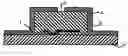
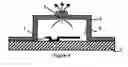
Conventionally, electromechanical Microsystems are enclosed in a hermetically-sealed microcavity delineated by a cover. A known method for production of a hermetic cover is represented in FIGS. 1 and 2. The electromechanical microsystems 1 are generally arranged on a substrate 2. As represented in FIG. 1, the cover is formed, on the substrate 2 and on a sacrificial layer 3 formed on the substrate 2, by a solid layer 4 in which a hole 5, or possibly several holes 5, is or are formed. Then the sacrificial layer 3 is removed via the hole 5 so as to obtain a microcavity 6, as represented in FIG. 2. Then a sealing layer 7 is deposited on the solid layer 4 forming the cover, so as to make the microcavity 6 hermetic.
Fabrication by means of a sacrificial layer 3 gives rise to two problems, among other, i.e. an insufficient tightness of sealing and a lengthy time required for the removal step of the sacrificial layer 3, in particular in the case of large covers 4.
To achieve hermetic sealing of the cover 4, the holes 5 are in fact typically small and localized in zones of the sacrificial layer 3, and consequently of the microcavity 6, that present a small thickness, as represented in FIG. 1. Typically, the thickness of the sacrificial layer 3 at the location of the hole 5, in a peripheral zone of the microcavity 6, is about 0.3 microns, whereas the thickness of the sacrificial layer 3 covering the electromechanical Microsystems 1 is about 10 microns. The etching step of the sacrificial layer 3 is then long and difficult. This drawback is all the more pronounced the smaller the thickness of the sacrificial layer 3 at the location of the hole 5, to achieve the best possible sealing, which thickness is sometimes less than 0.2 microns.
The document DE10005555 describes a microcomponent comprising a hermetic cavity delineated by a cover. The cover is formed by bottom and top layers respectively comprising holes offset with respect to one another. The holes of the top layer are sealed by closing layers, preferably made of aluminium, arranged on the bottom layer, under the holes. The bottom layer thus acts as continuous solid support for the sealing layers. When the sealing layers are made of aluminium, a temperature of 660° C. is applied to melt the sealing layers The sealing layers are located entirely above the top layer. The holes of the top layer are then filled by an additional sealing layer covering the top layer.
OBJECT OF THE INVENTIONIt is one object of the invention to remedy these shortcomings and, in particular, to achieve hermetic sealing of a microcavity while reducing the time required to produce the microcavity.
According to the invention, this object is achieved by the appended claims and in particular by the fact that the microcomponent comprises, under the sealing layer, a plug covering the hole and a part of the cover over the periphery of the hole, the plug being made from a material that is able to undergo creep deformation.
It is a further object of the invention to provide a method for production of a hermetically-sealed microcavity of a microcomponent, successively comprising
-
- deposition of a sacrificial layer on a substrate,
- deposition of a first layer forming a cover, on the substrate and sacrificial layer,
- etching, in the cover, of at least one hole opening out onto the sacrificial layer,
- removal of the sacrificial layer, via the hole, so as to create the microcavity,
- deposition of the sealing layer, so as to seal the microcavity hermetically,
method comprising deposition of the plug covering the hole and a part of the cover over the periphery of the hole, after the sacrificial layer has been removed and before the sealing layer is deposited.
Other advantages and features will become more clearly apparent from the following description of particular embodiments of the invention given as non-restrictive examples only and represented in the accompanying drawings, in which:
FIGS. 1 and 2 represent two steps of a method for production of a microcomponent according to the prior art.
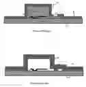
Les FIGS. 3 to 6 represent, in cross-section, four successive steps of a particular embodiment of a method for production of a microcomponent according to the invention.
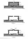
FIGS. 7 and 8 represent the step prior to deposition of the sealing layer of another particular embodiment of a method for production of a microcomponent according to the invention, respectively in top view and in cross-section along the line A-A.
FIG. 9 represents a pumping step of a particular embodiment of a method for production of a microcomponent according to the invention.
DESCRIPTION OF PARTICULAR EMBODIMENTSAs represented in FIGS. 3 and 4, the hole 5 etched in the cover 4 and opening out on the sacrificial layer 3 is preferably arranged on the highest part of the microcavity 6, i.e. at a location where the sacrificial layer 3 has a maximum thickness, for example about 8 to 10 microns. In this way, the duration of the subsequent creation step of the microcavity 6 by removal of the sacrificial layer 3, through the hole 5, represented in FIG. 4, is substantially reduced compared with the prior art.
In FIG. 5, a plug 8 is deposited, after the sacrificial layer 3 has been removed and before deposition of the sealing layer 9, so as to cover the hole 5 and a part of the cover 4 over the periphery of the hole 5. The plug 8 is made from a material that is able to undergo creep deformation. In a first embodiment, the material that is able to undergo creep deformation is a polymerized material, selected in particular from photoresist and polyimide. In a second embodiment, the material that is able to undergo creep deformation is a glass, selected in particular from phosphosilicate glasses. These materials seal the hole 5 without entering the microcavity 6. Moreover, these materials support the deposition conditions of the sealing layer 9 designed to seal the microcavity 6 hermetically, as represented in FIG. 6. The plug 8 preferably has a thickness comprised between 2 and 6 micrometers.
The plug can be achieved by deposition of a viscous polymer solution covering the cover 4, followed by etching of the layer thus obtained to delineate the plug 8 laterally.
It is well known that, for polymers, the temperatures applied during the method must not exceed 450° C. The use of polymers is then particularly suitable for methods performed at low temperature, i.e. methods having a maximum temperature comprised for example between 300° C. and 450° C., or even less.
In another embodiment the plug 8 can be produced by a method of the sol-gel type or by cathode sputtering, so as to obtain, for example, a phosphosilicate glass (PSG).
As represented in FIGS. 5 and 6, the plug 8 can have sloping sides 10, which improves the adhesion of the sealing layer 9 deposited on the plug 8, thus ensuring hermetic sealing without any risk of cracking.
To prevent the material forming the plug 8 from depositing inside the microcavity 6, the dimension of the hole 5 is preferably smaller than 5 micrometers. The hole 5 can for example have a substantially rectangular cross-section of 3 μm by 5 μm. As etching of the sacrificial layer 3 is slowed down by reduction of the size of the hole 5, the microcomponent preferably comprises a plurality of holes 5, in particular in the case of a cover 4 of large size. In FIGS. 7 and 8, for example, six holes 5 are arranged on two lines each comprising three holes 5. Each of the holes 5 is sealed by an associated plug 8 covering the corresponding hole 5 and a part of the cover 4 over the periphery of the hole 5, for example over a surface of 20 μm by 15 μm.
The plug 8 is not necessarily hermetic. In particular, the plug can be formed by a porous material, for example by a porous polymer. The porous material is, for example, a photoresist annealed at a temperature of more than 300° C. As illustrated in FIG. 9, a porous plug 8 enables gas contained in the microcavity 6 to be pumped through the porous material before the sealing layer 9 is deposited. This enables the pressure and nature of the gas inside the microcavity 6 to be controlled during the sealing step.
The material of the sacrificial layer 3 can be a polymer, for example polyimide or a photoresist, enabling rapid etching, for example dry etching, or a material obtained by a sol-gel type process. The cover 4 and sealing layer 9 can be made of silicon dioxide (SiO2), silicon nitride (Si3N4) or metal. The cover 4 can for example be achieved by deposition of silicon dioxide having, for example, a thickness of 1.5 microns. The sealing layer 9 is preferably achieved by deposition of silicon nitride having a thickness of 2 microns for example.
The invention is not limited to the particular embodiments represented. In particular, there can be any number of holes 5. A single layer forming several plugs 8 can if required be associated with several holes 5.
Claims
1-15. (canceled)
16. Microcomponent comprising a hermetically-sealed microcavity, delineated by a cover in which at least one hole is formed, and, on the cover, a sealing layer hermetically sealing the microcavity, the microcomponent comprising, under the sealing layer, a plug covering the hole and a part of the cover over the periphery of the hole, the sealing layer and the plug being formed by distinct materials, wherein the plug is made of a material that is able to undergo creep deformation.
17. Microcomponent according to claim 16, wherein the material that is able to undergo creep deformation is a polymerized material.
18. Microcomponent according to claim 17, wherein the polymerized material is selected from photoresists and polyimide.
19. Microcomponent according to claim 16, wherein the material that is able to undergo creep deformation is a glass.
20. Microcomponent according to claim 19, wherein the glass is selected from phosphosilicate glasses.
21. Microcomponent according to claim 16, wherein the dimension of the hole is smaller than 5 micrometers.
22. Microcomponent according to claim 16, wherein the hole is arranged on the highest part of the microcavity.
23. Microcomponent according to claim 16, comprising a plurality of holes.
24. Microcomponent according to claim 16, wherein the thickness of the plug is comprised between 2 and 6 micrometers.
25. Microcomponent according to claim 16, wherein the plug comprises sloping sides.
26. Microcomponent according to claim 16, wherein the plug is non-hermetical.
27. Microcomponent according to claim 16, wherein the material of the sealing layer is selected from silicon dioxide, silicon nitride and metals.
28. Method for production of a hermetically-sealed microcavity of a microcomponent according to claim 16, successively comprising
deposition of a sacrificial layer on a substrate,
deposition of a first layer forming the cover, on the substrate and sacrificial layer,
etching, in the cover, of at least one hole opening out onto the sacrificial layer,
removal of the sacrificial layer, via the hole, so as to create the microcavity,
deposition of the sealing layer, so as to seal the microcavity hermetically, method comprising deposition of the plug covering the hole and a part of the cover over the periphery of the hole, after the sacrificial layer has been removed and before the sealing layer is deposited.
29. Method according to claim 28, wherein, the plug is made of phosphosilicate glass, and the plug is obtained by a method selected from solgel methods and cathode sputtering.
30. Method according to claim 28, wherein the plug is made of a porous material.
31. Method according to claim 30, wherein, the porous material is a photoresist, and the method comprises a high temperature annealing step.
32. Method according to claim 30, wherein the method comprises a pumping step of the gas contained in the microcavity, through the porous material, before the sealing layer is deposited.
Images & Drawings included:
Sources:
- United States Patent and Trademark Office - verify current appl. status at the USPTO↗
Recent applications in this class:
- » 20250236513 2025-07-24
MEMS cavity with non-contaminating seal - » 20250197199 2025-06-19
PROCESS FOR MANUFACTURING MICROELECTROMECHANICAL DEVICES WITH CHAMBERS SEALED AT DIFFERENT PRESSURES AND MICROELECTROMECHANICAL DEVICE THEREBY MANUFACTURED - » 20250197198 2025-06-19
MANUFACTURING PROCESS FOR MICROELECTROMECHANICAL DEVICES HAVING IMPROVED SEALING PERFORMANCE - » 20240228267 2024-07-11
LASER SEALING METHODS FOR CLOSING VENTHOLES OF MICROMECAHNICAL DEVICES - » 20240132342 2024-04-25
LASER SEALING METHODS FOR CLOSING VENTHOLES OF MICROMECAHNICAL DEVICES - » 20240109771 2024-04-04
METHODS FOR SEALING CAVITIES IN MICRO-FABRICATED DEVICES AND MICRO-FABRICATED DEVICES FABRICATED IN ACCORDANCE WITH SAME - » 20230286798 2023-09-14
MEMS cavity with non-contaminating seal - » 20220162063 2022-05-26
MEMS cavity with non-contaminating seal - » 20210229985 2021-07-29
METHOD FOR MANUFACTURING MEMS DEVICE AND MEMS DEVICE - » 20200391997 2020-12-17
MEMS cavity with non-contaminating seal
Recent applications for this Assignee:
- » 20200088702 2020-03-19
Method of calibrating an electronic nose - » 20190096671 2019-03-28
Method of producing an element of a microelectronic device - » 20190047870 2019-02-14
Method for preparing silicon and/or germanium nanowires - » 20150365098 2015-12-17
Systems and methods for implementing error-shaping alias-free asynchronous flipping analog to digital conversion - » 20150050304 2015-02-19
CD4+ T survivin epitopes and uses thereof - » 20150034147 2015-02-05
Photovoltaic module comprising a localised spectral conversion element and production process - » 20150031580 2015-01-29
Method for the quantitative assessment of global and specific DNA repair capacities of at least one biological medium, and the applications therefor - » 20140341565 2014-11-20
Device for measurement of the profile of very short duration single pulses - » 20140241554 2014-08-28
Systems, devices, and methods for continuous-time digital signal processing and signal representation - » 20140231661 2014-08-21
Two-dimensional detection system for neutron radiation in the field of neutron scattering spectrometry