Photoelectric surface and photodetector
US20070132050A1
2007-06-14
11/511,497
2006-08-29
✅ Patent granted
US 7,525,131 B2
2009-04-28
-
-
Ida M Soward
2026-09-13
Abstract:
Disclosed is a photoelectric surface including: a first group III nitride semiconductor layer that produces photoelectrons according to incidence of ultraviolet rays; and a second group III nitride semiconductor layer provided adjacent to the first group III nitride semiconductor layer and made of a thin-film crystal having c-axis orientation in a thickness direction, the second group III nitride semiconductor layer having an Al composition higher than that of the first group III nitride semiconductor layer.
Inventors:
- Shunro FUKE 4 🇯🇵 Hamamatsu-shi, Japan
- Tokuaki NIHASHI 4 🇯🇵 Hamamatsu-shi, Japan
- Masatomo SUMIYA 3 🇯🇵 Tsukuba-shi, Japan
- Minoru HAGINO 3 🇯🇵 Hamamatsu-shi, Japan
- Masatomo Sumiya 3 🇯🇵 Tsukuba, Japan
- Shunro Fuke 6 🇯🇵 Hamamatsu, Japan
- Tokuaki Nihashi 3 🇯🇵 Hamamatsu, Japan
- Minoru Hagino 3 🇯🇵 Hamamatsu, Japan
Assignee:
- HAMAMATSU PHOTONICS K.K. 2,039 🇯🇵 Hamamatsu-shi, Shizuoka, Japan
- NATIONAL UNIVERSITY CORPORATION SHIZUOKA UNIVERSITY 23 🇯🇵 Shizuoka-shi ,Shizuoka, Japan
Interested in similar patents?
Get notified when new applications in this technology area are published.
Classification:
H01L33/00 IPC
Semiconductor devices with at least one potential-jump barrier or surface barrier specially adapted for light emission; Processes or apparatus specially adapted for the manufacture or treatment thereof or of parts thereof; Details thereof
H01L31/062 IPC
Semiconductor devices sensitive to infra-red radiation, light, electromagnetic radiation of shorter wavelength or corpuscular radiation and specially adapted either for the conversion of the energy of such radiation into electrical energy or for the control of electrical energy by such radiation; Processes or apparatus specially adapted for the manufacture or treatment thereof or of parts thereof; Details thereof adapted as photovoltaic [PV] conversion devices characterised by at least one potential-jump barrier or surface barrier the potential barriers being only of the metal-insulator-semiconductor type
H01L31/09 » CPC main
Semiconductor devices sensitive to infra-red radiation, light, electromagnetic radiation of shorter wavelength or corpuscular radiation and specially adapted either for the conversion of the energy of such radiation into electrical energy or for the control of electrical energy by such radiation; Processes or apparatus specially adapted for the manufacture or treatment thereof or of parts thereof; Details thereof in which radiation controls flow of current through the device, e.g. photoresistors Devices sensitive to infra-red, visible or ultraviolet radiation
H01L31/0304 » CPC further
Semiconductor devices sensitive to infra-red radiation, light, electromagnetic radiation of shorter wavelength or corpuscular radiation and specially adapted either for the conversion of the energy of such radiation into electrical energy or for the control of electrical energy by such radiation; Processes or apparatus specially adapted for the manufacture or treatment thereof or of parts thereof; Details thereof characterised by their semiconductor bodies characterised by the material; Inorganic materials including, apart from doping materials or other impurities, only AB compounds
H01J2201/3423 » CPC further
Electrodes common to discharge tubes; Photoemissive electrodes; Cathodes; Composition of the emitting surface Semiconductors, e.g. GaAs, NEA emitters
Y02E10/544 » CPC further
Energy generation through renewable energy sources; Photovoltaic [PV] energy Solar cells from Group III-V materials
Y02E10/544 » CPC further
Energy generation through renewable energy sources; Photovoltaic [PV] energy Solar cells from Group III-V materials
H01L27/14 IPC
Devices consisting of a plurality of semiconductor or other solid-state components formed in or on a common substrate including semiconductor components sensitive to infra-red radiation, light, electromagnetic radiation of shorter wavelength or corpuscular radiation and specially adapted either for the conversion of the energy of such radiation into electrical energy or for the control of electrical energy by such radiation
H01L29/732 IPC
Semiconductor devices adapted for rectifying, amplifying, oscillating or switching, or capacitors or resistors with at least one potential-jump barrier or surface barrier, e.g. PN junction depletion layer or carrier concentration layer; Details of semiconductor bodies or of electrodes thereof; Multistep manufacturing processes therefor; Types of semiconductor device ; Multistep manufacturing processes therefor controllable by only the electric current supplied, or only the electric potential applied, to an electrode which does not carry the current to be rectified, amplified or switched; Bipolar devices; Transistor-type devices, i.e. able to continuously respond to applied control signals; Bipolar junction transistors Vertical transistors
H01L31/0328 IPC
Semiconductor devices sensitive to infra-red radiation, light, electromagnetic radiation of shorter wavelength or corpuscular radiation and specially adapted either for the conversion of the energy of such radiation into electrical energy or for the control of electrical energy by such radiation; Processes or apparatus specially adapted for the manufacture or treatment thereof or of parts thereof; Details thereof characterised by their semiconductor bodies characterised by the material; Inorganic materials including, apart from doping materials or other impurities, semiconductor materials provided for in two or more of groups -
H01L31/0336 IPC
Semiconductor devices sensitive to infra-red radiation, light, electromagnetic radiation of shorter wavelength or corpuscular radiation and specially adapted either for the conversion of the energy of such radiation into electrical energy or for the control of electrical energy by such radiation; Processes or apparatus specially adapted for the manufacture or treatment thereof or of parts thereof; Details thereof characterised by their semiconductor bodies characterised by the material; Inorganic materials including, apart from doping materials or other impurities, semiconductor materials provided for in two or more of groups - in different semiconductor regions, e.g. CuX/CdX hetero-junctions, X being an element of Group VI of the Periodic System
H01L31/072 IPC
Semiconductor devices sensitive to infra-red radiation, light, electromagnetic radiation of shorter wavelength or corpuscular radiation and specially adapted either for the conversion of the energy of such radiation into electrical energy or for the control of electrical energy by such radiation; Processes or apparatus specially adapted for the manufacture or treatment thereof or of parts thereof; Details thereof adapted as photovoltaic [PV] conversion devices characterised by at least one potential-jump barrier or surface barrier the potential barriers being only of the PN heterojunction type
H01L31/109 IPC
Semiconductor devices sensitive to infra-red radiation, light, electromagnetic radiation of shorter wavelength or corpuscular radiation and specially adapted either for the conversion of the energy of such radiation into electrical energy or for the control of electrical energy by such radiation; Processes or apparatus specially adapted for the manufacture or treatment thereof or of parts thereof; Details thereof in which radiation controls flow of current through the device, e.g. photoresistors characterised by at least one potential-jump barrier or surface barrier, e.g. phototransistors; Devices sensitive to infra-red, visible or ultra-violet radiation characterised by only one potential barrier or surface barrier the potential barrier being of the PN heterojunction type
H01L29/06 IPC
Semiconductor devices adapted for rectifying, amplifying, oscillating or switching, or capacitors or resistors with at least one potential-jump barrier or surface barrier, e.g. PN junction depletion layer or carrier concentration layer; Details of semiconductor bodies or of electrodes thereof; Multistep manufacturing processes therefor; Semiconductor bodies ; Multistep manufacturing processes therefor characterised by their shape; characterised by the shapes, relative sizes, or dispositions of the semiconductor regions ; characterised by the concentration or distribution of impurities within semiconductor regions
H01L29/12 IPC
Semiconductor devices adapted for rectifying, amplifying, oscillating or switching, or capacitors or resistors with at least one potential-jump barrier or surface barrier, e.g. PN junction depletion layer or carrier concentration layer; Details of semiconductor bodies or of electrodes thereof; Multistep manufacturing processes therefor; Semiconductor bodies ; Multistep manufacturing processes therefor characterised by the materials of which they are formed
H01L29/04 IPC
Semiconductor devices adapted for rectifying, amplifying, oscillating or switching, or capacitors or resistors with at least one potential-jump barrier or surface barrier, e.g. PN junction depletion layer or carrier concentration layer; Details of semiconductor bodies or of electrodes thereof; Multistep manufacturing processes therefor; Semiconductor bodies ; Multistep manufacturing processes therefor characterised by their crystalline structure, e.g. polycrystalline, cubic or particular orientation of crystalline planes
H01L29/10 IPC
Semiconductor devices adapted for rectifying, amplifying, oscillating or switching, or capacitors or resistors with at least one potential-jump barrier or surface barrier, e.g. PN junction depletion layer or carrier concentration layer; Details of semiconductor bodies or of electrodes thereof; Multistep manufacturing processes therefor; Semiconductor bodies ; Multistep manufacturing processes therefor characterised by their shape; characterised by the shapes, relative sizes, or dispositions of the semiconductor regions ; characterised by the concentration or distribution of impurities within semiconductor regions with semiconductor regions connected to an electrode not carrying current to be rectified, amplified or switched and such electrode being part of a semiconductor device which comprises three or more electrodes
H01L31/036 IPC
Semiconductor devices sensitive to infra-red radiation, light, electromagnetic radiation of shorter wavelength or corpuscular radiation and specially adapted either for the conversion of the energy of such radiation into electrical energy or for the control of electrical energy by such radiation; Processes or apparatus specially adapted for the manufacture or treatment thereof or of parts thereof; Details thereof characterised by their semiconductor bodies characterised by their crystalline structure or particular orientation of the crystalline planes
H01L31/0376 IPC
Semiconductor devices sensitive to infra-red radiation, light, electromagnetic radiation of shorter wavelength or corpuscular radiation and specially adapted either for the conversion of the energy of such radiation into electrical energy or for the control of electrical energy by such radiation; Processes or apparatus specially adapted for the manufacture or treatment thereof or of parts thereof; Details thereof characterised by their semiconductor bodies characterised by their crystalline structure or particular orientation of the crystalline planes including amorphous semiconductors
H01L31/20 IPC
Semiconductor devices sensitive to infra-red radiation, light, electromagnetic radiation of shorter wavelength or corpuscular radiation and specially adapted either for the conversion of the energy of such radiation into electrical energy or for the control of electrical energy by such radiation; Processes or apparatus specially adapted for the manufacture or treatment thereof or of parts thereof; Details thereof; Processes or apparatus specially adapted for the manufacture or treatment of these devices or of parts thereof such devices or parts thereof comprising amorphous semiconductor materials
H01L27/15 IPC
Devices consisting of a plurality of semiconductor or other solid-state components formed in or on a common substrate including semiconductor components with at least one potential-jump barrier or surface barrier specially adapted for light emission
H01L29/74 IPC
Semiconductor devices adapted for rectifying, amplifying, oscillating or switching, or capacitors or resistors with at least one potential-jump barrier or surface barrier, e.g. PN junction depletion layer or carrier concentration layer; Details of semiconductor bodies or of electrodes thereof; Multistep manufacturing processes therefor; Types of semiconductor device ; Multistep manufacturing processes therefor controllable by only the electric current supplied, or only the electric potential applied, to an electrode which does not carry the current to be rectified, amplified or switched; Bipolar devices Thyristor-type devices, e.g. having four-zone regenerative action
H01L31/00 IPC
Semiconductor devices sensitive to infra-red radiation, light, electromagnetic radiation of shorter wavelength or corpuscular radiation and specially adapted either for the conversion of the energy of such radiation into electrical energy or for the control of electrical energy by such radiation; Processes or apparatus specially adapted for the manufacture or treatment thereof or of parts thereof; Details thereof
Description
BACKGROUND OF THE INVENTION1. Field of the Invention
The present invention relates to a photoelectric surface including a group III nitride semiconductor layer and a photodetector using the same.
2. Related Background Art
A photoelectric surface including a GaN layer as an active layer has been known (see Japanese Published Unexamined Patent Application No. H10-241554). In the photoelectric surface, when ultraviolet rays are made incident into the GaN layer, photoelectrons are emitted from the GaN layer.
SUMMARY OF THE INVENTIONEven in the aforementioned photoelectric surface, quantum efficiency when the GaN layer emits photoelectrons has been improved, however, a further improvement in quantum efficiency of the active layer has been demanded.
It is an object of the present invention to provide a photoelectric surface that is high in quantum efficiency and a photodetector using the same.
In order to solve the above-mentioned problems, a photoelectric surface according to the present invention includes: a first group III nitride semiconductor layer that produces photoelectrons according to incidence of ultraviolet rays; and a second group III nitride semiconductor layer provided adjacent to the first group III nitride semiconductor layer and made of a thin-film crystal having c-axis orientation in a thickness direction, the second group III nitride semiconductor layer having an Al composition higher than that of the first group III nitride semiconductor layer.
Here, the first group III nitride semiconductor layer may or may not contain Al.
A photoelectric surface according to the present invention includes: a first group III nitride semiconductor layer that produces photoelectrons according to incidence of ultraviolet rays; and a second group III nitride semiconductor layer provided adjacent to the first group III nitride semiconductor layer and polarized in a thickness direction.
A photodetector according to the present invention includes: the photoelectric surface; and an anode for extracting photoelectrons emitted from the photoelectric surface as an output signal.
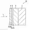
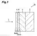
BRIEF DESCRIPTION OF THE DRAWINGSFIG. 1 is a sectional view schematically showing a photoelectric surface according to a first embodiment.
FIG. 2 shows a band model of the photoelectric surface shown in FIG. 1.
FIG. 3A to FIG. 3D are process sectional views schematically showing an example of a manufacturing method for the photoelectric surface according to the first embodiment, respectively.
FIG. 4 is a sectional view schematically showing a photodetector according to the first embodiment.
FIG. 5 is a sectional view schematically showing a photoelectric surface according to a second embodiment.
FIG. 6A to FIG. 6C are process sectional views schematically showing an example of a manufacturing method for the photoelectric surface according to the second embodiment, respectively.
FIG. 7A to FIG. 7E are process sectional views schematically showing an example of a manufacturing method for the photoelectric surface according to the second embodiment, respectively.
FIG. 8 is a sectional view schematically showing a photodetector according to the second embodiment.
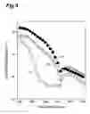
FIG. 9 is a graph showing a relationship between the wavelength of ultraviolet rays made incident into a photoelectric surface and quantum efficiency of the photoelectric surface.
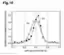
FIG. 10 is a graph showing a relationship between the energy distribution function and applied voltage.
DESCRIPTION OF THE PREFERRED EMBODIMENTSHereinafter, embodiments of the present invention will be described in detail with reference to the accompanying drawings. Here, in the description of the drawings, identical or equivalent elements are designated with identical numerical symbols so as to avoid overlapping descriptions.
First EmbodimentFIG. 1 is a sectional view schematically showing a photoelectric surface according to a first embodiment. FIG. 2 shows a band model of the photoelectric surface shown in FIG. 1. In FIG. 1, a reflective photoelectric surface 10 is shown. The photoelectric surface 10 includes a first group III nitride semiconductor layer (active layer) 8 that produces photoelectrons according to incidence of ultraviolet rays L and a second group III nitride semiconductor layer 6 provided adjacent to the group III nitride semiconductor layer 8. It is preferable that the group III nitride semiconductor layer 6 has a heterojunction with the group III nitride semiconductor layer 8.
It is preferable that the photoelectric surface 10 further includes a third group III nitride semiconductor layer 4. The group III nitride semiconductor layer 4 preferably contains Ga, and may contain Al, In, or the like. The group III nitride semiconductor layer 4 is, for example, AlxGal1-xN (0<x<1). It is preferable that the group III nitride semiconductor layer 4 is provided on a substrate 2. As the substrate 2, for example, a Si (111) substrate, a sapphire substrate, or the like having a thickness of 200 to 300 μm can be mentioned. The group III nitride semiconductor layer 6 is provided on the group III nitride semiconductor layer 4.
The group III nitride semiconductor layer 6 is made of a thin-film crystal having c-axis orientation in a thickness direction (crystal growth direction) and has an Al composition higher than that of the group III nitride semiconductor layer 8. The group III nitride semiconductor layer 6 has a first surface 6a and a second surface 6b. When the surface 6a is a +c surface (a surface in a positive c-polarity direction, a group III element surface forming compounds with nitrides), the surface 6b is a −c surface (a surface in a negative c-polarity direction, an N surface). When the surface 6a is a −c surface, the surface 6b is a +c surface.
The group III nitride semiconductor layer 6 is polarized in the thickness direction. It is preferable that a spontaneous polarization coefficient (for example, 0.09 C/m2 with AlN) of the group III nitride semiconductor layer 6 is greater than that (for example; 0.034 C/m2 with GaN) of the group III nitride semiconductor layer 8. Moreover, it is preferable that an energy band gap of the group III nitride semiconductor layer 6 is greater than that of the group III nitride semiconductor layer 8. Thereby, absorption of the ultraviolet rays L in the group III nitride semiconductor layer 6 can be prevented. If the Al composition of the group III nitride semiconductor layer 6 is increased, spontaneous polarization is enhanced and the energy band gap is also increased.
Since the group III nitride semiconductor layer 6 has the aforementioned configuration, an internal electric field occurs in the group III nitride semiconductor layer 6. The internal electric field occurs due to the above-mentioned spontaneous polarization of the group III nitride semiconductor layer 6 or a piezoelectric field caused by distortion (a distortion due to a tensile stress or a compressive stress) of the group III nitride semiconductor layer 6. The internal electric field resulting from spontaneous polarization reaches, for example, a few MV/cm. The distortion of the group III nitride semiconductor layer 6 occurs due to, for example, a difference in a lattice constant from the group III nitride semiconductor layer 4. If distortion polarization of the group III nitride semiconductor layer 6 increases, the internal electric field is also increased. The internal electric field concentrates in the vicinity of an interface between the group III nitride semiconductor layer 6 and group III nitride semiconductor layer 8 (a surface 8b of the group III nitride semiconductor layer 8 to be described later) due to a surface level.
The group III nitride semiconductor layer 6 preferably contains Ga, and may contain Al, In, or the like. The group III nitride semiconductor layer 6 is made from, for example, AlyGa1-yN (0<y≦1). The conductivity type of the group III nitride semiconductor layer 6 may be any of an n-type, a p-type, and an i-type. It is preferable that the group III nitride semiconductor layer 6 is made from a material different from that of the group III nitride semiconductor layer 4. In this case, by selecting an appropriate material, distortion polarization of the group III nitride semiconductor layer 6 can be controlled.
It is preferable that the thickness of the group III nitride semiconductor layer 6 is 3 to 100 nm. If the thickness of the group III nitride semiconductor layer 6 is less than 3 nm, crystallinity and flatness tend to be lowered. On the other hand, if the thickness of the group III nitride semiconductor layer 6 is more than 1.00 nm, the internal electric field of the group III nitride semiconductor layer 6 tends to be reduced.
The group III nitride semiconductor layer 8 preferably contains Ga, and may contain Al, In, or the like. When the group III nitride semiconductor layer 8 contains Al, by controlling the Al composition ratio, ultraviolet rays in a desired wavelength region of the ultraviolet rays L can be cut off. When the group III nitride semiconductor layer 8 contains In, the photoelectric surface 10 is favorably used for a sensor of long wavelength-side ultraviolet rays of the ultraviolet rays L. It is preferable that the group III nitride semiconductor layer 8 is made of a thin-film crystal. The conductivity type of the group III nitride semiconductor layer 8 may be either the n-type or p-type, and is preferably the same as the conductivity type of the group III nitride semiconductor layer 6. When the group III nitride semiconductor layer 8 contains Mg, a p-type group III nitride semiconductor layer 8 is obtained.
The group III nitride semiconductor layer 8 has a first surface 8a and a second surface 8b. It is preferable that the surface 8a is a −c surface (a surface in a negative c-polarity direction, an N surface). Thereby, photoelectrons are easily emitted from the group III nitride semiconductor layer 8. In this case, the surface 8b is a +c surface (a surface in a positive c-polarity direction, a group III element surface forming compounds with nitrides). When the surface 8a is a +c surface, the surface 8b is a −c surface.
It is preferable that the thickness of the group III nitride semiconductor layer 8 is 100 to 200 nm. If the thickness of the group III nitride semiconductor layer 8 is less than 100 nm, since crystal quality of the group III nitride semiconductor layer 8 is deteriorated, a quantum efficiency-enhancing effect tends to be lowered. On the other hand, if the thickness of the group III nitride semiconductor layer 8 is more than 200 nm, since the energy band is flattened by an increase in the number of carriers in the group III nitride semiconductor layer 8, a quantum efficiency-enhancing effect tends to be lowered.
It is preferable that the carrier concentration of the group III nitride semiconductor layer 8 is ×1015 to 1×1019 cm−3. If the carrier concentration of the group III nitride semiconductor layer 8 is less than 1×10¹⁵, fabrication of the group III nitride semiconductor layer 8 tends to be difficult. On the other hand, if the carrier concentration of the group III nitride semiconductor layer 8 is more than 1×10¹⁹, since energy band modulation by an internal electric field is limited to the vicinity of a surface, a quantum efficiency-enhancing effect tends to be lowered.
In the group III nitride semiconductor layer 8, it is preferable that the number of carriers (a product of the thickness and carrier concentration of the group III nitride semiconductor layer 8) per unit area is 1×10¹⁰ to 2×1014 cm−2.
For the photoelectric surface 10 of the present embodiment, an internal electric field occurs in the group III nitride semiconductor layer 6 due to, for example, a piezoelectric field caused by distortion or spontaneous polarization in the c-axis direction of the thin-film crystal. By the internal electric field, the energy band of the group III nitride semiconductor layer 8 is curved (see FIG. 2). When the group III nitride semiconductor layer 6 is made from AlN and the group III nitride semiconductor layer 8 is made from GaN, it is considered that an electric field of 0.66 V/nm is formed due to a difference in the spontaneous polarization coefficient. In this case, if the thickness of the group III nitride semiconductor layer 6 is provided as, for example, 3 nm, a rise in the energy band of 2 eV theoretically occurs in the group III nitride semiconductor layer 8. Note that 1 eV=1.602×10⁻¹⁹ J. When a rise in the energy band occurs, surface potential of the surface 8a of the group III nitride semiconductor layer 8 is modulated. When the ultraviolet rays L are made incident into such a group III nitride semiconductor layer 8, photoelectrons produced in the group III nitride semiconductor layer 8 are easily emitted outside from the group III nitride semiconductor layer 8. Consequently, quantum efficiency of the photoelectric surface 10 can be improved.
In addition, when the photoelectric surface 10 includes the group III nitride semiconductor layer 4, crystal quality of the group III nitride semiconductor layer 6 can be improved compared to when the group III nitride semiconductor layer 6 is directly formed on the substrate 2. When the group III nitride semiconductor layer 4 is thickened, crystal quality of the group III nitride semiconductor layer 6 can further be improved. In addition, layer thickness uniformity and flatness of the group III nitride semiconductor layer 6 are improved. As a result, crystal quality of the group III nitride semiconductor layer 8 can be improved. Consequently, quantum efficiency of the photoelectric surface 10 can further be improved.
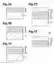
FIG. 3A to FIG. 3D are process sectional views schematically showing an example of a manufacturing method for the photoelectric surface 10, respectively. First, as shown in FIG. 3A, the substrate 2 is prepared. And, as shown in FIG. 3B, the group III nitride semiconductor layer 4 is formed on the substrate 2. Furthermore, as shown in FIG. 3C, the group III nitride semiconductor layer 6 is formed on the group III nitride semiconductor layer 4. Then, as shown in FIG. 3D, the group III nitride semiconductor layer 8 is formed on the group III nitride semiconductor layer 6. The group III nitride semiconductor layers 4, 6, and 8 are formed by epitaxial growth by use of, for example, an MOCVD apparatus. In this manner, the photoelectric surface 10 with a high quantum efficiency is obtained.
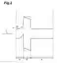
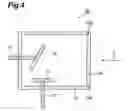
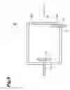
FIG. 4 is a sectional view schematically showing a photodetector according to the present embodiment. A photodetector 20 shown in FIG. 4 includes the photoelectric surface 10 and an anode 14 for extracting photoelectrons emitted from the photoelectric surface 10 as an output signal. The photoelectric surface 10 and anode 14 are arranged in a chamber 12. As the photodetector 20, for example, a phototube or the like can be mentioned.
The interior of the chamber 12 is maintained in a vacuum by use of, for example, a pump. To an end portion 12a of the chamber 12, an entrance window 18 for introducing the ultraviolet rays L into the chamber 12 is connected. By the entrance window 18, the interior of the chamber 12 is sealed. The anode 14 is electrically connected to a lead wire 16. The photoelectric surface 10 is electrically connected to a lead wire 17. In the photodetector 20, since quantum efficiency of the photoelectric surface 10 can be improved, the ultraviolet rays L can be detected at a high sensitivity.
A spontaneous emission of a flame includes short-wavelength ultraviolet rays not included in sunlight or indoor lighting. By using the photodetector 20, the short-wavelength ultraviolet rays can be selectively and efficiently detected. In addition, since the photoelectric surface 10 is formed mainly of a nitride based semiconductor material, photoelectric properties are favorably maintained even in a high-temperature operating environment. Therefore, the photodetector 20 can be favorably used as a flame sensor for a refuse incinerator, a gas range, or the like.
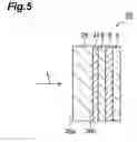
Second EmbodimentFIG. 5 is a sectional view schematically showing a photoelectric surface according to a second embodiment. In FIG. 5, a transmissive photoelectric surface 30 is shown. The photoelectric surface 30 includes, similar to the photoelectric surface 10, the group III nitride semiconductor layers 6 and 8. Accordingly, in the photoelectric surface 30 as well, quantum efficiency can be improved.
It is preferable that the photoelectric surface 30 further includes a glass substrate 26 into whose one surface 26a ultraviolet rays L are made incident and an adhesive layer 24 provided on the other surface 26b opposed to the surface 26a of the glass substrate 26 and arranged between the glass substrate 26 and group III nitride semiconductor layer 6. Between the group III nitride semiconductor layer 6 and adhesive layer 24, a protective layer 9 for protecting the group III nitride semiconductor layers 6 and 8 may be provided as necessary. The protective layer 9 is made of, for example, a group III nitride semiconductor.
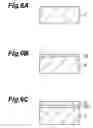
FIG. 6A to FIG. 6C and FIG. 7A to FIG. 7E are process sectional views schematically showing an example of a manufacturing method for the photoelectric surface 30, respectively. First, as shown in FIG. 6A, the substrate 2 is prepared. And, as shown in FIG. 6B, a buffer layer 22 is formed on the substrate 2. By use of, for example, an MOCVD apparatus, the buffer layer 22 can be formed on the substrate 2. Furthermore, as shown in FIG. 6C, the group III nitride semiconductor layer 8 is on the buffer layer 22. Then, as shown in FIG. 7A, the group III nitride semiconductor layer 6 is formed on the group III nitride semiconductor layer 8. Next, as shown in FIG. 7B, the protective layer 9 is formed on the group III nitride semiconductor layer 6 as necessary. The group III nitride semiconductor layers 6 and 8 and protective layer 9 are formed by epitaxial growth by use of, for example, an MOCVD apparatus. Next, as shown in FIG. 7C, the adhesive layer 24 is formed on the protective layer 9. Next, as shown in FIG. 7D, the glass substrate 26 is placed on the adhesive layer 24. Then, by removing the substrate 2 and buffer layer 22 by, for example, wet etching, the photoelectric surface 30 shown in FIG. 7E is obtained.
FIG. 8 is a sectional view schematically showing a photodetector according to the present embodiment. A photodetector 40 shown in FIG. 8 includes the photoelectric surface 30 and the anode 14 for extracting photoelectrons emitted from the photoelectric surface 30 as an output signal. The anode 14 is arranged in the chamber 12. As the photodetector 40, for example, a phototube or the like can be mentioned.
The interior of the chamber 12 is maintained in a vacuum by use of, for example, a pump. To the end portion 12a of the chamber 12, the photoelectric surface 30 into which the ultraviolet rays L are made incident is connected. By the photoelectric surface 30, the interior of the chamber 12 is sealed. The anode 14 is electrically connected to the lead wire 16. The photoelectric surface 30 is electrically connected to the lead wire 17. In the photodetector 40, since quantum efficiency of the photoelectric surface 30 can be improved, the ultraviolet rays L can be detected at a high sensitivity.
Moreover, since use of the photodetector 40 allows two-dimensional imaging, refuse can be efficiently disposed of in, for example, a refuse incinerator. As a result, dioxin emissions can be suppressed.
In the above, preferred embodiments of the present invention have been described in detail, however, the present invention is by no means limited to the embodiments described above.
Hereinafter, the present invention will be described in greater detail based on examples and comparative examples, however, the present invention is not limited to the following examples.
EXAMPLE 1First, a GaN base layer (group III nitride semiconductor layer 4) having a thickness of 600 nm was formed on a sapphire substrate (substrate 2). Furthermore, under a reduced pressure (76 Torr), an AlN layer (group III nitride semiconductor layer 6) having a thickness of 100 nm was formed on the GaN base layer. Note that 1 Torr=133.322 Pa. Thereafter, a GaN active layer (group III nitride semiconductor layer 8) having a thickness of 200 nm was formed on the AlN layer. In this manner, a photoelectric surface of Example 1 was obtained.
EXAMPLE 2Except that the thickness of the AlN layer was provided as 50 nm and the thickness of the GaN active layer was provided as 100 nm, in the same manner as in Example 1, a photoelectric surface of Example 2 was obtained.
COMPARATIVE EXAMPLE 1After a GaN buffer layer having a thickness of 20 nm was formed on a sapphire substrate, a GaN active layer having a thickness of 300 nm was formed on the GaN buffer layer. In this manner, a photoelectric surface of Comparative Example 1 was obtained.
Evaluation Results
Quantum efficiency in relation to each wavelength was measured for the photoelectric surfaces of Examples 1 and 2 and Comparative Examples 1.
FIG. 9 is a graph showing a relationship between the wavelength of ultraviolet rays made incident into a photoelectric surface and quantum efficiency of the photoelectric surface. The horizontal axis of the graph shows a wavelength (nm) of ultraviolet rays. The vertical axis of the graph shows quantum efficiency (%) of a photoelectric surface. In the graph of FIG. 9, data D1 and D2 show measurement results of Examples 1 and 2, respectively, and data C1 shows a measurement result of Comparative Example 1. It is understood from the graph that quantum efficiency of the photoelectric surface of Examples 1 and 2 is higher than that of Comparative Example 1. This indicates that such an electric field that electrons photoexcited on the surface (surface 8b) by depletion in the vicinity of the AlN layer-side surface (surface 8b) of the GaN active layer are accelerated toward the surface (surface 8a) has been formed.
FIG. 10 is a graph showing a relationship between the energy distribution function and applied voltage. The horizontal axis of the graph shows an applied voltage (V). The vertical axis of the graph shows an energy distribution function (relative value). The energy distribution function is obtained by differentiating a photocurrent obtained when an extraction voltage is provided as −10V to +20V by use of a low-pressure mercury lamp that provides a 10 mm-diameter circle with energy of 1 μW. Data E1 shows a measurement result of a GaN thin film having a thickness of 300 nm whose front surface is a Ga surface. Data E2 shows a measurement result of a GaN thin film having a thickness of 300 nm whose front surface is an N surface. In the data E1, it shows a peak at +0.1V, while in the data E2, it shows a peak at −1.0 to 0V. Therefore, it is understood that the GaN thin film whose front surface is an N surface more easily emits photoelectrons. When the GaN thin film whose front surface is an N surface and the GaN thin film whose front surface is a G surface both have the same photoelectron emission rate, the difference in the peak position indicates a difference in the surface potential barrier. By a calculation without regard for the surface level, since holes are accumulated in the Ga surface, the difference in the surface potential between the Ga surface and N surface equals 3 eV. However, in actuality, accumulation of holes in the Ga surface is replaced by accumulation of positive electric charges at the surface level, and does not become such a great difference as 3 eV.
As has been described above, according to the present invention, a photoelectric surface that is high in photon efficiency and a photodetector using the same are provided.
Claims
What is claimed is:1. A photoelectric surface comprising:
a first group III nitride semiconductor layer that produces photoelectrons according to incidence of ultraviolet rays; and
a second group III nitride semiconductor layer provided adjacent to the first group HI nitride semiconductor layer and made of a thin-film crystal having c-axis orientation in a thickness direction, the second group III nitride semiconductor layer having an Al composition higher than that of the first group III nitride semiconductor layer.
2. The photoelectric surface according to claim 1, further comprising a third group III nitride semiconductor layer, wherein the second group III nitride semiconductor layer is provided on the third group III nitride semiconductor layer.
3. The photoelectric surface according to claim 1, further comprising:
a glass substrate into whose one surface ultraviolet rays are made incident; and
an adhesive layer provided on the other surface opposed to the surface of the glass substrate and arranged between the glass substrate and the second group III nitride semiconductor layer.
4. A photoelectric surface comprising:
a first group III nitride semiconductor layer that produces photoelectrons according to incidence of ultraviolet rays; and
a second group III nitride semiconductor layer provided adjacent to the first group III nitride semiconductor layer and are polarized in a thickness direction.
5. A photodetector comprising:
the photoelectric surface according to claim 1; and
an anode for extracting photoelectrons emitted from the photoelectric surface as an output signal.
6. A photodetector comprising:
the photoelectric surface according to claim 4; and
an anode for extracting photoelectrons emitted from the photoelectric surface as an output signal.
Images & Drawings included:
Sources:
- United States Patent and Trademark Office - verify current appl. status at the USPTO↗
Recent applications in this class:
- » 20240234614 2024-07-11
ULTRAVIOLET SENSOR - » 20240222541 2024-07-04
PHOTOCONDUCTIVE SWITCH WITH DIAMOND - » 20240145612 2024-05-02
SEMICONDUCTOR SYSTEM WITH WAVEGUIDE ASSEMBLY WITH RF SIGNAL IMPEDANCE CONTROLLABLE BY APPLIED, etc. - » 20240097064 2024-03-21
LOW RESISTANCE PHOTOCONDUCTIVE SEMICONDUCTOR SWITCH (PCSS) - » 20230411548 2023-12-21
PHOTOCONDUCTOR AND METHOD FOR PRODUCING SAME - » 20230361235 2023-11-09
HEAT BLOCKING DEVICE, HEAT BLOCKING FILM, AND HEAT BLOCKING COMPOSITION - » 20230275176 2023-08-31
PHOTON DETECTOR ARRAY ASSEMBLY - » 20220231181 2022-07-21
Photodetection element, receiving device, and optical sensor device - » 20220093811 2022-03-24
Optical sensor and detector for an optical detection - » 20210376179 2021-12-02
Photon detector array assembly
Recent applications for this Assignee:
- » 20250287721 2025-09-11
SEMICONDUCTOR LIGHT-RECEIVING ELEMENT - » 20250264738 2025-08-21
DATA CREATION DEVICE, OPTICAL CONTROL DEVICE, TARGET INTENSITY SPECTROGRAM CREATION DEVICE, DATA CREATION METHOD, TARGET INTENSITY SPECTROGRAM CREATION METHOD, DATA CREATION PROGRAM, AND TARGET INTENSITY SPECTROGRAM CREATION PROGRAM - » 20250258306 2025-08-14
LIGHT DETECTION DEVICE - » 20250258039 2025-08-14
SPECTROSCOPY DEVICE, RAMAN SPECTROSCOPIC MEASUREMENT DEVICE, AND SPECTROSCOPY METHOD - » 20250253620 2025-08-07
LIGHT SOURCE DEVICE AND CONTROL METHOD - » 20250244491 2025-07-31
RADIATION DETECTOR AND RADIATION DETECTION DEVICE - » 20250244172 2025-07-31
SPECTROMETRY DEVICE - » 20250244123 2025-07-31
THICKNESS-DISTRIBUTION MEASUREMENT DEVICE AND THICKNESS-DISTRIBUTION MEASUREMENT METHO - » 20250241604 2025-07-31
HEAD IMAGE ACQUISITION DEVICE AND HEAD IMAGE ACQUISITION METHOD - » 20250231386 2025-07-17
MICROSCOPE AND IMAGE PROCESSING METHOD