Variable gain amplifier
US20070132513A1
2007-06-14
11/497,461
2006-08-01
✅ Patent granted
US 7,348,849 B2
2008-03-25
-
-
Benny Lee | Alan Wong
2026-11-02
Abstract:
A complementary metal oxide semiconductor (CMOS) variable gain amplifier has a wider decibel-linear gain variation characteristic with respect to a control voltage when a signal is amplified. The variable gain amplifier includes: a bias input circuit for supplying a current corresponding to a bias voltage; an operation region combination and feedback circuit connected to the bias input circuit and combining at least two amplifiers by feedback in response to a control voltage, each amplifier having a decibel-linear characteristic in saturation and triode regions of a complementary metal oxide semiconductor (CMOS); and a bias output circuit connected to the bias input circuit, and outputting bias current controlled by the operation region combination and feedback circuit.
Inventors:
- Hyun Kyu YU 70 🇰🇷 Daejeon, South Korea
- Seon-Ho HAN 26 🇰🇷 Daejeon, South Korea
- Hyun Kyu Yu 8 🇰🇷 Daejon, South Korea
Assignee:
- Electronics and Telecommunications Research Institute 12,929 🇰🇷 Daejeon, South Korea
Interested in similar patents?
Get notified when new applications in this technology area are published.
Classification:
H03G1/007 » CPC main
Details of arrangements for controlling amplification; Circuits characterised by the type of controlling devices operated by a controlling current or voltage signal using continuously variable impedance elements using FET type devices
H03F1/342 » CPC further
Details of amplifiers with only discharge tubes, only semiconductor devices or only unspecified devices as amplifying elements; Negative-feedback-circuit arrangements with or without positive feedback in field-effect transistor amplifiers
H03F3/211 » CPC further
Amplifiers with only discharge tubes or only semiconductor devices as amplifying elements; Power amplifiers, e.g. Class B amplifiers, Class C amplifiers with semiconductor devices only using a combination of several amplifiers
H03F3/45206 » CPC further
Amplifiers with only discharge tubes or only semiconductor devices as amplifying elements; Differential amplifiers with semiconductor devices only characterised by the way of implementation of the active amplifying circuit in the differential amplifier using MOSFET transistors as the active amplifying circuit; Pl types Folded cascode stages
H03G7/06 » CPC further
Volume compression or expansion in amplifiers having semiconductor devices
H03F2200/15 » CPC further
Indexing scheme relating to amplifiers the supply or bias voltage or current at the drain side of a FET being continuously controlled by a controlling signal
H03F2203/21154 » CPC further
Indexing scheme relating to amplifiers with only discharge tubes or only semiconductor devices as amplifying elements covered by; Indexing scheme relating to power amplifiers, e.g. Class B amplifiers, Class C amplifiers with semiconductor devices only using a combination of several amplifiers An output signal of a power amplifier being controlled by controlling voltage signal
H03F2203/45008 » CPC further
Indexing scheme relating to amplifiers with only discharge tubes or only semiconductor devices as amplifying elements covered by; Indexing scheme relating to differential amplifiers the addition of two signals being made by a resistor addition circuit for producing the common mode signal
H03F2203/45302 » CPC further
Indexing scheme relating to amplifiers with only discharge tubes or only semiconductor devices as amplifying elements covered by; Indexing scheme relating to differential amplifiers the common gate stage of a cascode dif amp being controlled
H03F3/45 IPC
Amplifiers with only discharge tubes or only semiconductor devices as amplifying elements Differential amplifiers
H03G3/10 IPC
Gain control in amplifiers or frequency changers without distortion of the input signal; Manually-operated control in untuned amplifiers having semiconductor devices
Description
CROSS-REFERENCE TO RELATED APPLICATIONThis application claims priority to and the benefit of Korean Patent Application No. 2005-121442, filed Dec. 12, 2005, the disclosure of which is incorporated herein by reference in its entirety.
BACKGROUND1. Field of the Invention
The present invention relates to a variable gain amplifier (VGA), and more particularly, to a complementary metal oxide semiconductor (CMOS) variable gain amplifier having a wider variable gain range than a conventional VGA in the same control voltage variation range.
2. Discussion of Related Art
In general, in a radio frequency (RF) communication transceiver, a receiver has a variable gain amplifier for producing, according to the magnitude of an input signal, a constant signal-to-noise (SNR) characteristic. The variable gain amplifier allows the input signal, whose magnitude in decibels (dB) varies with a distance, to fix the magnitude of a final analog signal of the receiver. Further, the variable gain amplifier serves to provide decibel-linear gain variation with a control voltage in order to make a time taken to perform automatic gain control (AGC) uniform.
An example of the conventional variable gain amplifier is a variable gain amplifier using a bipolar junction transistor (BJT). Owing to the BJT, the variable gain amplifier represents an exponential characteristic of output current depending on input voltage and accordingly, has the advantage of easily obtaining linear-in-dB variable gain.
Another example of the conventional variable gain amplifier is a variable gain amplifier using a complementary metal oxide semiconductor (CMOS). The CMOS variable gain amplifier represents a square law characteristic in which radio frequency input power from a noise level to a −20 dB level is proportional to the square of small signal voltage. Therefore, the CMOS variable gain amplifier generally has a circuit for obtaining a pseudo decibel-linear gain characteristic. However, unlike the variable gain amplifier using the BJT, the CMOS variable gain amplifier has many transistors, and thus has a complicated circuit, high current consumption, a large noise factor, and a considerably large design area.
SUMMARYThe present invention is directed to a complementary metal oxide semiconductor (CMOS) variable gain amplifier, which combines an operation region of the amplifier varied between a saturation region and a triode region while forming a feedback loop within a combination circuit, thereby providing a wider variable gain range in the same control voltage variation range, reducing current consumption, improving a noise factor, and considerably reducing a design area, compared to a conventional CMOS variable gain amplifier.
One aspect of the present invention provides a variable gain amplifier comprising: a bias input circuit for supplying a current corresponding to a bias voltage; an operation region combination and feedback circuit connected to the bias input circuit and combining at least two amplifiers by feedback in response to a control voltage, each amplifier having a decibel-linear characteristic in saturation and triode regions of a complementary metal oxide semiconductor (CMOS); and a bias output circuit connected to the bias input circuit, and outputting bias current controlled by the operation region combination and feedback circuit.
The bias input circuit may comprise a first transistor operating in the saturation region, and having a control terminal to which the bias voltage is applied, a first terminal to which a predetermined voltage is applied, and a second terminal connected to the operation region combination and feedback circuit and the bias output circuit. The operation region combination and feedback circuit may comprise a second transistor having a first terminal to which the current is applied, a control terminal to which the control voltage is applied, and a second terminal; and a third transistor having a first terminal connected to the second terminal of the first transistor, a second terminal, and a control terminal connected to the first terminal of the first transistor. The amplifier may use a current rate in the saturation regions of the first and second transistors, and provide operation and feedback in the triode region using the third transistor.
In the variable gain amplifier, when increase of the control voltage generates a section in which an operation region of the second transistor is in the saturation region and a section in which an operation region of the third transistor is in the triode region, a total gain (Avp) may vary depending on variation of linear control voltage in the following equation:
Avp(dB)≈(−β−α)·Vc
where β is the slope of decibel-linear gain versus control voltage when there is no third transistor and the second transistor operates in the saturation region, and α is the slope of decibel-linear transconductance of the third transistor versus control voltage.
The variable gain amplifier may further comprise a bias control unit, for example, a resistor connected to the second terminal of the third transistor.
The bias output circuit may comprise a fourth transistor having a first terminal, a second terminal, and a control terminal. The first terminal may be connected to the second terminal of the first transistor and the first terminal of the second transistor, and an input signal may be input to the control terminal.
Another aspect of the present invention provides a variable gain amplifier having a differential structure.
BRIEF DESCRIPTION OF THE DRAWINGSThe above and other features and advantages of the present invention will become more apparent by describing in detail preferred embodiments thereof with reference to the attached drawings in which:
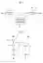
FIG. 1 is a block diagram illustrating a basic construction of a CMOS variable gain amplifier according to the present invention;
FIG. 2 is a circuit diagram of a CMOS variable gain amplifier according to an exemplary embodiment of the present invention;
FIG. 3 is a graph showing a simulation result of direct current (DC) characteristics in the circuit of FIG. 2;
FIG. 4 is a graph showing a simulation result of variable gain characteristics versus control voltage in the circuit of FIG. 2; and
FIG. 5 is a circuit diagram illustrating a CMOS variable gain amplifier of a differential structure according to another exemplary embodiment of the present invention.
DETAILED DESCRIPTION OF PREFERRED EMBODIMENTSHereinafter, exemplary embodiments of the present invention will be described in detail. However, the present invention is not limited to the exemplary embodiments disclosed below, and can be implemented in various modified forms. Therefore, the present exemplary embodiments are provided for complete disclosure of the present invention and to fully inform the scope of the present invention to those of ordinary skill in the art.
FIG. 1 is a block diagram illustrating a basic construction of a complementary metal oxide semiconductor (CMOS) variable gain amplifier according to the present invention.
Basically, the linear-in-dB CMOS variable gain amplifier according to the present invention is to obtain a wider variable gain range by combination of a principle of obtaining a decibel-linear characteristic in a saturation region and a principle of obtaining a decibel-linear characteristic in a triode region. Compared to a conventional CMOS variable gain amplifier, the CMOS variable gain amplifier according to the present invention obtains the wider variable gain range, thereby reducing current consumption, improving a noise factor, and considerably reducing a design area. In the CMOS variable gain amplifier according to the present invention, feedback is a medium for obtaining the wide variable gain range through combination of the triode region and the saturation region. Such a construction is schematically shown in FIG. 1. As illustrated in FIG. 1, the CMOS variable gain amplifier according to the present invention includes a bias input circuit 11 for inputting a bias voltage (VBias), an operation region combination and feedback circuit 12 for combining the saturation region with the triode region of a transistor by a control voltage (Vc), and forming an operation region of the amplifier, and a bias output circuit 13 for outputting current bias whose gain is controlled depending on the voltage bias in response to an input signal (Vin).
FIG. 2 is a circuit diagram of a CMOS variable gain amplifier according to an exemplary embodiment of the present invention.
Referring to FIG. 2, the CMOS variable gain amplifier according to the present invention has a simple structure including four transistors, one of which is a P-type MOS transistor Q1 and the others are N-type MOS transistors Q2, Q3, and Q4.
Specifically, the first transistor Q1 includes a first terminal, a second terminal, and a control terminal. The first terminal is connected to a power source having a predetermined voltage (Vdd), and the bias voltage (VBias) is applied to the control terminal. The first transistor Q1 serves as the bias input circuit 11 for inputting the bias voltage (VBias).
The second transistor Q2 includes a first terminal, a second terminal, and a control terminal. The first terminal is connected to the second terminal of the first transistor Q1, and the control voltage (Vc) is applied to the control terminal. The third transistor Q3 includes a first terminal, a second terminal, and a control terminal. The first terminal is connected to the second terminal of the second transistor Q2. The second terminal is connected to one terminal of a resistor R for optimal bias control. The control terminal is commonly connected to the second terminal of the first transistor Q1 and the first terminal of the second transistor Q2. With the above-mentioned configuration, the second and third transistors Q2 and Q3 serve as the operation region combination and feedback circuit 12 operating in the saturation and triode regions respectively, in response to the control voltage (Vc).
The fourth transistor Q4 includes a first terminal, a second terminal, and a control terminal. The first terminal is commonly connected to the second terminal of the first transistor Q1, the first terminal of the second transistor Q2, and the control terminal of the third transistor Q3. The second terminal is connected to an input terminal of a current source (IBias), and the input signal (Vin) is applied to the control terminal. Owing to the above configuration, the fourth transistor Q4 serves as the bias output circuit 13 for outputting the bias current (IBias) whose gain is controlled by the operation region combination and feedback circuit 12 depending on the bias voltage (VBias), in response to the input signal (Vin). The resistor R serves as a bias control unit 14 that optimally controls bias in a whole circuit obtaining the decibel-linear characteristic.
An operation of the above-described CMOS variable gain amplifier will be described below. First, if the bias voltage (VBias) is applied to the control terminal of the first transistor Q1, the first transistor Q1 of a PMOS type operates in the saturation region, and transmits current corresponding to the bias voltage (VBias). If the control voltage (Vc) is applied to the control terminal of the second transistor Q2, the second transistor Q2 is varied in the operation region by the control voltage (Vc). For example, when the control voltage (Vc) is varied from a high level to a low level, the second transistor Q2 is varied in its operation region from the saturation region to the triode region. The third transistor Q3 is varied in its operation region from the triode region to the saturation region depending on variation of the control voltage (Vc), and its output voltage is fedback and applied to a gate. In view of an output node, the output voltage forms a voltage-current feedback loop.
FIG. 3 is a graph showing a simulation result of direct current (DC) characteristics in the circuit of FIG. 2.
As shown in FIG. 3, operation regions of the two transistors Q2 and Q3 within the operation region combination and feedback circuit are varied from the saturation region to the triode region or from the triode region to the saturation region depending on the variation of the control voltage (Vc).
Typical output resistance (Rout) represents output resistance upon variation of the control voltage (Vc), and is provided as decibel-linear output resistance to the control voltage (Vc). This is to not only use a current rate in two saturation regions but also obtain a pseudo linear-in-dB gain characteristic by approximation of Equation 1 using the current rate in the two saturation regions.
exp(2nx)≈((1+x)/(1−x))n [Equation 1]
Here, transconductance (Gm) of the third transistor Q3 is expressed as shown in FIG. 3. In other words, when the bias resistance (R) varies depending on the variation of the control voltage (Vc), the transconductance (Gm) of the third transistor Q3 also has a decibel-linear gain characteristic proportional to a certain constant (α). As such, the variable gain amplifier represents the decibel-linear gain characteristic in the triode region.
FIG. 4 is a graph showing a simulation result of variable gain characteristics versus control voltage in the circuit of FIG. 2.
As shown in FIG. 4, the gain (Av) characteristic is approximately expressed by product of the control voltage and −β in a decibel-linear range. This represents a gain caused by decibel-linear output resistance when using two kinds of current of the saturation regions of two transistors Q2 and Q3 of the operation region combination and feedback circuit 12 of FIG. 2. Due to the feedback, the gain (Av) characteristic is divided by the transconductance (Gm) of the third transistor Q3. The transconductance (Gm) of the third transistor Q3 has the decibel-linear gain characteristic in the triode region. Accordingly, a final gain (Avp) of the circuit of FIG. 2 is expressed as in Equation 2. In other words, slope of total gain variation versus same control voltage variation range is increased due to the feedback, thereby increasing a linear-in-dB gain range.
Avp(dB)≈(−β−α)·Vc [Equation 2]
where β is the slope of decibel-linear gain versus control voltage when there is no third transistor and the second transistor operates in the saturation region, and α is the slope of decibel-linear transconductance of the third transistor versus control voltage.
It can be also appreciated that there is the decibel-linear gain variation when the resistance (R) is varied in FIG. 4.
FIG. 5 is a circuit diagram illustrating a CMOS variable gain amplifier of a differential structure according to another exemplary embodiment of the present invention.
Referring to FIG. 5, the CMOS variable gain amplifier having the differential structure includes two PMOS transistors M1 and M2 and eight NMOS transistors M3 to M10, and the variable gain amplifier circuit of FIG. 2 can be differentially embodied.
The first and second transistors M1 and M2 each include a first terminal, a second terminal, and a control terminal. The first terminals are connected to both terminals of a first resistor R1, respectively. The respective second terminals are commonly connected to a ground. The bias voltage (VBias) is commonly connected to the respective control terminals. Basically, the first resistor R1 is to improve linearity of a process signal in the differential structured circuit. When a resistor of the differential structured circuit is substituted using a metal oxide semiconductor (MOS), the gain can be discretely controlled as well.
The third and fourth transistors M3 and M4 each include a first terminal, a second terminal, and a control terminal. The second terminals are connected to the first terminals of the first and second transistors M1 and M2, respectively. Two input signals (IN+ and IN−) are applied to the control terminals, respectively.
The fifth and sixth transistors M5 and M6 each include a first terminal, a second terminal, and a control terminal. The first terminals are commonly connected to the power source having the predetermined voltage (Vdd). The second terminals are connected to the first terminals of the third and fourth transistors M3 and M4, respectively. The respective control terminals are commonly connected with each other. A second resistor R2 is connected between the control terminal and the second terminal of the third transistor M3. A third resistor R3 is connected between the control terminal and the second terminal of the fourth transistor M4. The second and third resistors R2 and R3 for common mode negative feedback set self-output bias voltages.
The seventh and eighth transistors M7 and M8 each include a first terminal, a second terminal, and a control terminal. The first terminals are connected to the second terminals of the fifth and sixth transistors M5 and M6, respectively. The respective control terminals are commonly connected with each other, and the control voltage (Vc) is commonly applied to the respective control terminals.
The ninth and tenth transistors M9 and M10 each include a first terminal, a second terminal, and a control terminal. The first terminals are connected to the second terminals of the seventh and eighth transistors M7 and M8, respectively. The second terminals are commonly connected to one terminal of the fourth resistor R4. The control terminals are connected to a connection point of the third and fifth transistors M3 and M5 and a connection point of the fourth and sixth transistors M4 and M6, respectively. The fourth resistor R4 serves to control the bias in the whole circuit obtaining the decibel-linear characteristic. The connection point of the third and fifth transistors M3 and M5 and the connection point of the fourth and sixth transistors M4 and M6 are two output points (OUT+ and OUT−).
Among the first to tenth transistors, the fifth and sixth transistors are PMOS transistors, and the first to fourth transistors and the seventh to tenth transistors are NMOS transistors.
The variable gain amplifier according to the second exemplary embodiment of the present invention has great advantageous effect of eliminating the common mode noise, compared to the variable gain amplifier according to the first exemplary embodiment of the present invention.
As described above, the variable gain amplifier according to the present invention can have the wider variable gain range for the same control voltage variation range, provide low current consumption, improve the noise factor, and embody a simple structure in which the design area is considerably reduced, compared to the conventional CMOS variable gain amplifier.
While the invention has been shown and described with reference to certain exemplary embodiments thereof, it will be understood by those skilled in the art that various changes in form and details may be made therein without departing from the spirit and scope of the invention as defined by the appended claims.
Claims
What is claimed is:1. A variable gain amplifier comprising:
a bias input circuit for supplying a current corresponding to a bias voltage;
an operation region combination and feedback circuit connected to the bias input circuit and combining at least two amplifiers by feedback in response to a control voltage, each amplifier having a decibel-linear characteristic in saturation and triode regions of a complementary metal oxide semiconductor (CMOS); and
a bias output circuit connected to the bias input circuit, and outputting bias current controlled by the operation region combination and feedback circuit.
2. The amplifier according to claim 1, wherein the bias input circuit comprises a first transistor operating in the saturation region, and having a control terminal to which the bias voltage is applied, a first terminal to which a predetermined voltage is applied, and a second terminal connected to the operation region combination and feedback circuit and the bias output circuit.
3. The amplifier according to claim 2, wherein the operation region combination and feedback circuit comprises:
a second transistor having a first terminal to which the current is applied, a control terminal to which the control voltage is applied, and a second terminal; and
a third transistor having a first terminal connected to the second terminal of the first transistor, a second terminal, and a control terminal connected to the first terminal of the first transistor.
4. The amplifier according to claim 3, wherein the amplifier makes use of a current rate in the saturation regions of the first and second transistors, and provides operation and feedback in the triode region using the third transistor.
5. The amplifier according to claim 3, wherein, when increase of the control voltage generates a section in which an operation region of the second transistor is in the saturation region and a section in which an operation region of the third transistor is in the triode region, a total gain (Avp) varies depending on variation of linear control voltage in the following equation:
Avp(dB)≈(−β−α)·Vc
where β is the slope of decibel-linear gain versus control voltage when there is no third transistor and the second transistor operates in the saturation region, and α is the slope of decibel-linear transconductance of the third transistor versus control voltage.
6. The amplifier according to claim 3, further comprising a bias control unit connected to the second terminal of the third transistor.
7. The amplifier according to claim 6, wherein the bias control unit is a resistor.
8. The amplifier according to claim 3, wherein the bias output circuit comprises a fourth transistor having a first terminal, a second terminal, and a control terminal, the first terminal being connected to the second terminal of the first transistor and the first terminal of the second transistor, and an input signal being input to the control terminal.
9. The amplifier according to claim 3, wherein the amplifier has a differential structure.
Images & Drawings included:


Sources:
- United States Patent and Trademark Office - verify current appl. status at the USPTO↗
Similar patent applications:
- » 20070273435
AM intermediate frequency variable gain amplifier circuit, variable gain amplifier circuit and its semiconductor integrated circuit - » 20070126501
Variable gain amplifier and variable gain amplifier module - » 20060284671
Variable gain amplifier circuit, method of correcting DC offset of the variable gain amplifying circuit, and radio receiving apparatus - » 20240322761
AUTO CALIBRATION CIRCUIT, VARIABLE GAIN AMPLIFIER AND AUTO CALIBRATION METHOD FOR CALIBRATING OUTPUT VOLTAGES OF THE VARIABLE GAIN AMPLIFIER - » 20090072903
Variable gain amplifier having variable gain DC offset loop - » 20140320207
Low noise variable gain amplifier utilizing variable feedback techniques with constant input/output impedance - » 20160149022
Heterojunction field effect transistor (HFET) variable gain amplifier having variable transconductance - » 20120242408
Low noise variable gain amplifier utilizing variable feedback techniques with constant input/output impedance - » 20080238542
Variable gain amplifier and method for achieving variable gain amplification with high bandwidth and linearity - » 20080258814
Variable gain amplifier and method for achieving variable gain amplification with high bandwidth and linearity
Recent applications in this class:
- » 20230231525 2023-07-20
Variable gain amplifier circuit and method having linearity compensation mechanism - » 20220052663 2022-02-17
Semiconductor device, electronic device, and artificial satellite - » 20210344316 2021-11-04
Field effect transistor circuits - » 20200382087 2020-12-03
Variable gain amplifier - » 20200177145 2020-06-04
Biasing circuits for voltage controlled or output circuits - » 20190214953 2019-07-11
High linearly WiGig baseband amplifier with channel select filter - » 20180287577 2018-10-04
Open-loop linear VGA - » 20180191321 2018-07-05
Temperature-compensated equalizer - » 20180131338 2018-05-10
Variable attenuation device, phase-switching variable attenuation device, and phase shifter - » 20180097489 2018-04-05
High linearly WiGig baseband amplifier with channel select filter
Recent applications for this Assignee:
- » 20250294796 2025-09-18
GATE ALL AROUND FIELD EFFECT TRANSISTOR HAVING MULTIPLE GATE STACK STRUCTURE AND FABRICATION METHOD THEREFOR - » 20250294275 2025-09-18
APPARATUS AND METHOD FOR ACQUIRING DATA SYNCHRONIZATION IN PASSIVE OPTICAL NETWORK - » 20250292130 2025-09-18
APPARATUS AND METHOD FOR SIMULATING LOGICAL QUBIT - » 20250292122 2025-09-18
APPARATUS AND METHOD FOR DISTRIBUTED MULTI-AGENT REINFORCEMENT LEARNING - » 20250292078 2025-09-18
METHOD AND APPARATUS FOR GENERATING NEURAL NETWORK MODELS FOR MISSING VALUE RESTORATION - » 20250288888 2025-09-18
METHOD FOR REAL-TIME INTERACTIVE DANCE EDUCATION USING AVATAR AND APPARATUS THEREFOR - » 20250287310 2025-09-11
APPARATUS AND METHOD FOR MONITORING RADIO RESOURCE IN MULTI-NETWORK ENVIRONMENT - » 20250287000 2025-09-11
METHOD AND APPARATUS FOR TRANSFORM-BASED IMAGE ENCODING/DECODING - » 20250286925 2025-09-11
MOBILE DEVICE AND SELECTIVE OFFLOADING METHOD OF THE SAME - » 20250286883 2025-09-11
APPARATUS AND METHOD FOR MANAGING CLOUD COMPUTING INFRASTRUCTURE ACCESS BASED ON DYNAMIC PARALLEL NODES