Semiconductor structure
US20070145007A1
2007-06-28
11/706,201
2007-02-15
Abstract:
This invention relates to a semiconductor structure for dual damascene processing and includes upper and lower low k dielectric layers formed in a stack when the upper surface of the lower layer has an integral etch stop layer formed by exposing the upper surfaces of the layer H2 plasma without any prior anneal prior to the deposition of the upper layer.
Inventors:
- Keith Edward Buchanan 1 🇬🇧 Trellech, United Kingdom
- Joon-Chai Yeoh 1 🇬🇧 Blackwood, United Kingdom
Interested in similar patents?
Get notified when new applications in this technology area are published.
Classification:
H01L21/76826 » CPC main
Processes or apparatus adapted for the manufacture or treatment of semiconductor or solid state devices or of parts thereof; Manufacture or treatment of devices consisting of a plurality of solid state components formed in or on a common substrate or of parts thereof; Manufacture of integrated circuit devices or of parts thereof; Manufacture of specific parts of devices defined in group; Applying interconnections to be used for carrying current between separate components within a device comprising conductors and dielectrics characterised by the formation and the after-treatment of the dielectrics, e.g. smoothing; Modification of the material of dielectric layers, e.g. grading, after-treatment to improve the stability of the layers, to increase their density etc. by contacting the layer with gases, liquids or plasmas
H01L21/76807 » CPC further
Processes or apparatus adapted for the manufacture or treatment of semiconductor or solid state devices or of parts thereof; Manufacture or treatment of devices consisting of a plurality of solid state components formed in or on a common substrate or of parts thereof; Manufacture of integrated circuit devices or of parts thereof; Manufacture of specific parts of devices defined in group; Applying interconnections to be used for carrying current between separate components within a device comprising conductors and dielectrics characterised by the formation and the after-treatment of the dielectrics, e.g. smoothing by forming openings in dielectrics for dual damascene structures
H01L21/76822 » CPC further
Processes or apparatus adapted for the manufacture or treatment of semiconductor or solid state devices or of parts thereof; Manufacture or treatment of devices consisting of a plurality of solid state components formed in or on a common substrate or of parts thereof; Manufacture of integrated circuit devices or of parts thereof; Manufacture of specific parts of devices defined in group; Applying interconnections to be used for carrying current between separate components within a device comprising conductors and dielectrics characterised by the formation and the after-treatment of the dielectrics, e.g. smoothing Modification of the material of dielectric layers, e.g. grading, after-treatment to improve the stability of the layers, to increase their density etc.
H01L21/76829 » CPC further
Processes or apparatus adapted for the manufacture or treatment of semiconductor or solid state devices or of parts thereof; Manufacture or treatment of devices consisting of a plurality of solid state components formed in or on a common substrate or of parts thereof; Manufacture of integrated circuit devices or of parts thereof; Manufacture of specific parts of devices defined in group; Applying interconnections to be used for carrying current between separate components within a device comprising conductors and dielectrics characterised by the formation and the after-treatment of the dielectrics, e.g. smoothing characterised by the formation of thin functional dielectric layers, e.g. dielectric etch-stop, barrier, capping or liner layers
H01L21/302 IPC
Processes or apparatus adapted for the manufacture or treatment of semiconductor or solid state devices or of parts thereof; Manufacture or treatment of semiconductor devices or of parts thereof the devices having at least one potential-jump barrier or surface barrier, e.g. PN junction, depletion layer or carrier concentration layer the devices having semiconductor bodies comprising elements of Group IV of the Periodic System or AB compounds with or without impurities, e.g. doping materials; Treatment of semiconductor bodies using processes or apparatus not provided for in groups - to change their surface-physical characteristics or shape, e.g. etching, polishing, cutting
C23F1/00 IPC
Etching metallic material by chemical means
H01L21/461 IPC
Processes or apparatus adapted for the manufacture or treatment of semiconductor or solid state devices or of parts thereof; Manufacture or treatment of semiconductor devices or of parts thereof the devices having at least one potential-jump barrier or surface barrier, e.g. PN junction, depletion layer or carrier concentration layer the devices having semiconductor bodies not provided for in groups, , , and with or without impurities, e.g. doping materials; Treatment of semiconductor bodies using processes or apparatus not provided for in groups to change their surface-physical characteristics or shape, e.g. etching, polishing, cutting
Description
CROSS-REFERENCE TO RELATED APPLICATIONThis is a divisional of application Ser. No. 10/484,168, filed Jan. 20, 2004, which is incorporated herein by reference in its entirety.
BACKGROUNDThis invention relates to a semiconductor structure for dual damascene processing.
Damascene processing is becoming particularly important in the formation of semiconductor devices, because it is the method which is most suited to the deposition of copper. In order to perform damascene processing it is necessary to etch different, but overlapping, structures into stacked layers of dielectric by successive etch processes and this is best achieved when it is possible to detect when the etch has reached the boundary between two layers in a stack. In order for this stage to be detected, it is typical to form an etch stop layer at the boundary and this is typically done by depositing a thin layer of silicon nitride or carbide between the two dielectric layers. These materials have relatively high dielectric constants and add both to the thickness of the device and the dielectric constant of the dielectric stack.
SUMMARYThe present invention consists in a semiconductor structure suitable for dual damascene processing including upper and lower low dielectric constant (k) dielectric layers formed in a stack wherein the upper surface of the lower layer has an integral etch stop layer formed by exposing the upper surface of the layer to H2 plasma without any prior anneal, prior to the deposition of the upper layer.
The material of at least the lower dielectric layer may be of SiCHO type material and may for example be formed by reacting tetramethylsilane and oxygen.
It is preferred that the etch stop layer is less than 1000 Å thick and is formed coincidentally with the lower dielectric layer and thus not consuming any additional process resources of time, materials or equipment over that required to fully form the dielectric layer.
From another aspect the invention consists in a method of etching dielectric layers including utilizing a surface layer formed by H2 plasma treatment of a SiCHO type material low k dielectric as an etch stop layer.
The etching may form part of a dual damascene process.
Although the invention has been defined above it is to be understood it includes any inventive combination of the features set out above or in the following description.
BRIEF DESCRIPTION OF THE DRAWINGSThe invention may be performed in various ways and will now be described, by way of example, with reference to the accompanying drawings, in which:
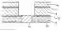
FIG. 1 is a scrap cross-section showing the prior art arrangement for dual damascene processing;
FIG. 2 is an equivalent view illustrating the process of the invention;
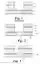
FIG. 3 is a view corresponding to FIG. 2, but wherein the etch elements have become partially offset; and
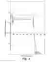
FIG. 4 is a SIM profile for a TMS and O2 deposited film which has been set with a 5 minute H2 plasma.
DETAILED DESCRIPTIONIn FIG. 1 a dual damascene structure has been etched on a semiconducting or insulating wafer. Thus a metalised via at 1 is bordered by a low dielectric constant insulating layer 2 having an etch stop layer 3 on its surface. This stop layer has the function or providing a stop for a trench etch process. The etch stop layer is then subsequently sputter etched removed from the top of the metal in the via to allow subsequent metal in the trench to contact it. The trench has been etched in a low dielectric constant insulator 4 using a mask 5. Typically layers 2 and 4 are essentially the same materials and are frequently bounded by other layers such as barrier layer 6 and capping layer 7.
One example of the invention is illustrated in FIG. 2. A via filled with metal or organic plug 1a formed in a low dielectric constant insulating layer 8 may be present—though not necessarily so. The precise sequence of when the via is etched and filled with metal is not important to the need for an etch stop layer for the formation of the overlaying trench. This layer may have a barrier layer 6a. A second dielectric layer 9 is provided as in the prior art as is a mask 5a.
In the applicants' International Patent Application WO 01/01472, which is incorporated herein by reference, a method of forming a low k dielectric material by reacting tetramethylsilane and oxygen and subsequently treating it with H2 plasma is described. In FIG. 19 of that document, which is hereby reproduced as FIG. 4, it was shown that such a film had a surface layer which was chemically different to the bulk of the layer. At the time, the applicants assumed that they would remove that layer so as to achieve a consistent dielectric material, but in any event that, for dual damascene and related processes, they would have to provide the convention etch stop layer. The applicants have now determined that this surface layer or curst can be utilized as an etch stop layer. Thus in FIG. 2 the curst portion, which is indicated at 16, FIG. 4, forms the integral etch stop layer 10 for dielectric layer 8 and can indeed constitute a capping layer 11 for the dielectric constant layer 9.
A typical treatment to create such an etch stop layer would be a hydrogen plasma treatment consisting of a 400° C. platen, 4 torr pressure, 1000 sccm of H2 and 1 kw applied at 13.56 MHz to an upper showerhead electrode. Typically pure hydrogen has been used by hydrogen mixed with inert carrier gases or hydrogen containing gases may be suitable.
Whilst trench etch has been described here, via etching onto a trench may also be improved by a surface layer of the invention, for example if the via mask is mis-aligned as illustrated in FIG. 3. In this case a metalised trench 12 has a via 13 etched to make a contact. If properly aligned and bordered this via etch would terminate on the trench metal completely, but if it is mis-aligned the via etch will need to terminate on a mix of trench metal and trench insulating layer 14. It can readily be seen that if a surface modification of the trench insulating layer upper surface 15 has been carried out to form an integral etch stop surface then the via etch will be improved. Thus the surface modification of the trench insulating layer will assist in via etches tolerating mis-alignment of the via mask and thus increase wafer yields.
Claims
What is claimed is:1. A method of etching dielectric layers comprising utilizing a surface layer formed by H2 plasma treatment of a SiCHO type material low k dielectric as an etch stop layer.
2. The method as claimed in claim 2 wherein the etching forms part of a damascene process.
Images & Drawings included:
Sources:
- United States Patent and Trademark Office - verify current appl. status at the USPTO↗
Similar patent applications:
- » 20240404825
METHODS OF MAKING SEMICONDUCTOR STRUCTURES, SEMICONDUCTOR STRUCTURES, AND SEMICONDUCTOR PROCESSING SYSTEMS AND COMPUTER PROGRAM PRODUCTS FOR MAKING SEMICONDUCTOR STRUCTURES - » 20150357521
Nitride semiconductor structure, electronic device including the nitride semiconductor structure, light-emitting device including the nitride semiconductor structure, and method for producing the nitride semiconductor structure - » 20250167144
SEMICONDUCTOR STRUCTURE, SEMICONDUCTOR CHIP INCLUDING SEMICONDUCTOR STRUCTURE AND METHOD FOR MANUFACTURING SEMICONDUCTOR STRUCTURE - » 20130307031
Semiconductor structure, semiconductor device having a semiconductor structure, and method for manufacturing a semiconductor structure - » 20230157008
METHOD FOR MANUFACTURING SEMICONDUCTOR STRUCTURE, SEMICONDUCTOR STRUCTURE, AND SEMICONDUCTOR MEMORY - » 20230061322
Method for manufacturing semiconductor structure, semiconductor structure and semiconductor memory - » 20220084966
BONDING PAD STRUCTURE, SEMICONDUCTOR STRUCTURE, SEMICONDUCTOR PACKAGE STRUCTURE AND METHOD FOR PREPARING SAME - » 20230011180
METHOD FOR MANUFACTURING SEMICONDUCTOR STRUCTURE, SEMICONDUCTOR STRUCTURE AND SEMICONDUCTOR MEMORY - » 20230028597
PREPARATION METHOD FOR SEMICONDUCTOR STRUCTURE, SEMICONDUCTOR STRUCTURE AND SEMICONDUCTOR MEMORY - » 20230032102
Method for manufacturing semiconductor structure, semiconductor structure and semiconductor memory
Recent applications in this class:
- » 20250069948 2025-02-27
DEPOSITION OF METALS IN RECESSED FEATURES WITH THE USE OF HALOGEN-CONTAINING DEPOSITION INHIBITORS - » 20240404876 2024-12-05
SEMICONDUCTOR DEVICES AND METHODS OF MANUFACTURE - » 20240395607 2024-11-28
ETCH PROFILE CONTROL OF GATE CONTACT OPENING - » 20240047267 2024-02-08
TUNGSTEN GAP FILL WITH HYDROGEN PLASMA TREATMENT - » 20230377955 2023-11-23
ELECTRON MIGRATION CONTROL IN INTERCONNECT STRUCTURES - » 20230369105 2023-11-16
Method for manufacturing semiconductor device comprising contact void surrounding bit line - » 20230369104 2023-11-16
Method for manfacturing semiconductor device for reducing partcle-induced defects - » 20230335434 2023-10-19
THERMAL PROCESS CHAMBER LID WITH BACKSIDE PUMPING - » 20230298934 2023-09-21
Etch profile control of gate contact opening - » 20230238278 2023-07-27
Manufacturing method of package structure of electronic device