Image sensor module with passive component
US20070145569A1
2007-06-28
11/317,071
2005-12-22
✅ Patent granted
US 7,368,795 B2
2008-05-06
-
-
Jasmine Clark
2026-05-25
Abstract:
An image sensor module with passive component includes a flexible print circuit board having an upper surface, which is formed with a plurality of electrically circuits, and a lower surface. At least a passive component is arranged on the upper surface of the flexible circuit board. A substrate has a first surface, a second surface, and a penetrated hole. The second surface of the substrate is mounted on the upper surface of the flexible circuit board, so that the passive component is located within the penetrated hole. A chip is mounted on the first surface of the substrate, and is located onto the penetrated hole of the substrate. A plurality of wires are electrically connected the chip to the substrate. A lens holder is mounted on first surface of the substrate, and is formed with an internal thread. And a lens barrel is formed with an external thread screwed on the internal thread of the lens holder, the lens barrel formed with an opening, an aspheric lens, and an infrared filter.
Assignee:
- Kingpak Technology Inc. 23 🇹🇼 Hsinchu Hsien, Taiwan
Interested in similar patents?
Get notified when new applications in this technology area are published.
Classification:
H01L23/02 IPC
Details of semiconductor or other solid state devices Containers; Seals
H01L27/14618 » CPC main
Devices consisting of a plurality of semiconductor or other solid-state components formed in or on a common substrate including semiconductor components sensitive to infra-red radiation, light, electromagnetic radiation of shorter wavelength or corpuscular radiation and specially adapted either for the conversion of the energy of such radiation into electrical energy or for the control of electrical energy by such radiation; Devices controlled by radiation; Imager structures; Structural or functional details thereof Containers
H01L25/167 » CPC further
Assemblies consisting of a plurality of individual semiconductor or other solid state devices ; Multistep manufacturing processes thereof the devices being of types provided for in two or more different main groups of - , e.g. forming hybrid circuits comprising optoelectronic devices, e.g. LED, photodiodes
H01L27/14625 » CPC further
Devices consisting of a plurality of semiconductor or other solid-state components formed in or on a common substrate including semiconductor components sensitive to infra-red radiation, light, electromagnetic radiation of shorter wavelength or corpuscular radiation and specially adapted either for the conversion of the energy of such radiation into electrical energy or for the control of electrical energy by such radiation; Devices controlled by radiation; Imager structures; Structural or functional details thereof Optical elements or arrangements associated with the device
H01L27/14636 » CPC further
Devices consisting of a plurality of semiconductor or other solid-state components formed in or on a common substrate including semiconductor components sensitive to infra-red radiation, light, electromagnetic radiation of shorter wavelength or corpuscular radiation and specially adapted either for the conversion of the energy of such radiation into electrical energy or for the control of electrical energy by such radiation; Devices controlled by radiation; Imager structures; Structural or functional details thereof Interconnect structures
H01L31/0203 » CPC further
Semiconductor devices sensitive to infra-red radiation, light, electromagnetic radiation of shorter wavelength or corpuscular radiation and specially adapted either for the conversion of the energy of such radiation into electrical energy or for the control of electrical energy by such radiation; Processes or apparatus specially adapted for the manufacture or treatment thereof or of parts thereof; Details thereof; Details Containers; Encapsulations, e.g. encapsulation of photodiodes
H01L31/02162 » CPC further
Semiconductor devices sensitive to infra-red radiation, light, electromagnetic radiation of shorter wavelength or corpuscular radiation and specially adapted either for the conversion of the energy of such radiation into electrical energy or for the control of electrical energy by such radiation; Processes or apparatus specially adapted for the manufacture or treatment thereof or of parts thereof; Details thereof; Details; Coatings for devices characterised by at least one potential jump barrier or surface barrier for filtering or shielding light, e.g. multicolour filters for photodetectors
H01L31/0232 » CPC further
Semiconductor devices sensitive to infra-red radiation, light, electromagnetic radiation of shorter wavelength or corpuscular radiation and specially adapted either for the conversion of the energy of such radiation into electrical energy or for the control of electrical energy by such radiation; Processes or apparatus specially adapted for the manufacture or treatment thereof or of parts thereof; Details thereof; Details Optical elements or arrangements associated with the device
H01L2924/15153 » CPC further
Indexing scheme for arrangements or methods for connecting or disconnecting semiconductor or solid-state bodies as covered by; Details of package parts other than the semiconductor or other solid state devices to be connected; Die mounting substrate; Shape the die mounting substrate comprising a recess for hosting the device
H01L2924/1517 » CPC further
Indexing scheme for arrangements or methods for connecting or disconnecting semiconductor or solid-state bodies as covered by; Details of package parts other than the semiconductor or other solid state devices to be connected; Die mounting substrate Multilayer substrate
H01L2924/16195 » CPC further
Indexing scheme for arrangements or methods for connecting or disconnecting semiconductor or solid-state bodies as covered by; Details of package parts other than the semiconductor or other solid state devices to be connected; Cap; Shape Flat cap [not enclosing an internal cavity]
H01L2924/19103 » CPC further
Indexing scheme for arrangements or methods for connecting or disconnecting semiconductor or solid-state bodies as covered by; Details of hybrid assemblies other than the semiconductor or other solid state devices to be connected; Disposition of discrete passive components in a stacked assembly with the semiconductor or solid state device interposed between the semiconductor or solid-state device and the die mounting substrate, i.e. chip-on-passive
H05K1/189 » CPC further
Printed circuits; Printed circuits structurally associated with non-printed electric components characterised by the use of a flexible or folded printed circuit
H05K1/189 » CPC further
Printed circuits; Printed circuits structurally associated with non-printed electric components characterised by the use of a flexible or folded printed circuit
H05K2201/10515 » CPC further
Indexing scheme relating to printed circuits covered by; Details of components or other objects attached to or integrated in a printed circuit board; Details of mounted components; Involving several components Stacked components
H05K2201/10515 » CPC further
Indexing scheme relating to printed circuits covered by; Details of components or other objects attached to or integrated in a printed circuit board; Details of mounted components; Involving several components Stacked components
H01L2924/00014 » CPC further
Indexing scheme for arrangements or methods for connecting or disconnecting semiconductor or solid-state bodies as covered by; Technical content checked by a classifier the subject-matter covered by the group, the symbol of which is combined with the symbol of this group, being disclosed without further technical details
H01L23/12 IPC
Details of semiconductor or other solid state devices Mountings, e.g. non-detachable insulating substrates
H01L27/14 IPC
Devices consisting of a plurality of semiconductor or other solid-state components formed in or on a common substrate including semiconductor components sensitive to infra-red radiation, light, electromagnetic radiation of shorter wavelength or corpuscular radiation and specially adapted either for the conversion of the energy of such radiation into electrical energy or for the control of electrical energy by such radiation
Description
BACKGROUND OF THE INVENTION1. Field of the Invention
The invention relates an image sensor module with passive component, and particular to a structure for packaging image sensor module, the size of the package may be decreased, and the manufacturing cost may be decreased.
2. Description of the Related Art
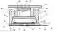
Referring to FIG. 1, it is an image sensor module structure includes a substrate 10, frame layer 18, a chip 26, a plurality of wires 28, transparent layer 34, a lens holder 35 and a lens barrel 46.
The substrate 10 has an first surface 12 on which plurality of first electrodes 15 are formed, and a second surface 14 on which plurality of second electrodes 16 are formed, the first electrodes 15 are corresponding to electrically connect to the second electrodes 16.
The frame layer 18 has a upper surface 20 and a lower surface 22, the lower surface 22 of the frame layer 18 is adhered on the first surface 22 of the substrate 10 to form a cavity 24.
The chip 26 is arranged on the first surface 12 of the substrate 10, and is located within the cavity 24, and is formed with bonding pads 27.
The wire 28 has a first end 30 and a second end 32, the first end 30 is electrically connected the bonding pad 27 of the chip 26, the second end 30 is electrically connected the first electrodes 15 of the substrate 10.
The transparent layer 34 is adhered on the upper surface 20 of the frame layer 18.
The lens holder 35 has an upper end surface 36, a lower end surface 40, and a penetrated region 42, which is formed with internal thread 44.
The lens barrel 46 is formed with external thread 39 screwed on the internal thread 44 of the lens holder 35, an opening 47, an aspheric lens 481, and an infrared filter 49.
Please refer to FIG. 2, the substrate 10 is mounted on a flexible print board 55, the second electrodes 16 of the substrate 10 are electrically connected to the flexible print board 55, which is formed with passive component 57, therefore, the module is used to connect to a electrical device by the flexible print board 55.
SUMMARY OF THE INVENTIONAn objective of the invention is to provide an image sensor module with passive component, and capable of decreasing the size of the module.
Another objective of the invention is to provide an image sensor module with passive component, and capable of increasing the reliability of the module.
To achieve the above-mentioned object, the invention includes a flexible print circuit board having an upper surface, which is formed with a plurality of electrically circuits, and a lower surface. At least a passive component is arranged on the upper surface of the flexible circuit board. A substrate has a first surface, a second surface, and a penetrated hole. The second surface of the substrate is mounted on the upper surface of the flexible circuit board, so that the passive component is located within the penetrated hole. A chip is mounted on the first surface of the substrate, and is located onto the penetrated hole of the substrate. A plurality of wires are electrically connected the chip to the substrate. A lens holder is mounted on first surface of the substrate, and is formed with an internal thread. And a lens barrel is formed with an external thread screwed on the internal thread of the lens holder, the lens barrel formed with an opening, an aspheric lens, and an infrared filter.
BRIEF DESCRIPTION OF THE DRAWINGSFIG. 1 is a cross-sectional view illustration showing a conventional image sensor module package.
FIG. 2 is a schematic illustration showing a conventional image sensor module package.
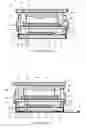
FIG. 3 is a first illustration showing an image sensor module with passive component of the present invention.
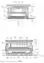
FIG. 4 is a second illustration showing an image sensor module with passive component of the present invention.
DETAILED DESCRIPTION OF THE INVENTIONPlease refer to FIG. 3, an image sensor module with passive component includes a flexible print board 50, passive component 51, substrate 52,a chip 54, wires 56, a lens holder 50, and a lens barrel 60.
The flexible print circuit board 50 has an upper surface 62, which is formed with a plurality of electrically circuits 66, and a lower surface 61.
The passive component 51 is arranged on the upper surface 62 of the flexible circuit board 50, and is electrically connected to the electrically circuits 66 of the flexible circuit board 50.
The substrate 52 has a first surface 68, a second surface 70, and a penetrated hole 72, the first surface 68 is formed with first electrodes 74, the second surface 70 is formed with second electrodes 76, the second surface 70 of the substrate 52 is mounted on the upper surface 62 of the flexible circuit board 50, and the second electrodes 76 of the substrate 52 are electrically connected the electrically circuit 66 of the flexible print circuit board 50, so that the passive component 51 is located within the penetrated hole 72.
The chip 54 is mounted on the first surface 68 of the substrate 52, and is located onto the penetrated hole 72 of the substrate 52. The chip 54 is formed with bonding pads 78.
The plurality of wires 56 are electrically connected the bonding pads 78 of the chip 54 to the first electrodes 74 of the substrate 52.
The lens holder 58 is mounted on first surface 68 of the substrate 52 to surround the chip 54, and is formed with an internal thread 80. And
The lens barrel 60 is formed with an external thread 82 screwed on the internal thread o80 f the lens holder 58, the lens barrel 60 is formed with an opening 84, an aspheric lens 86, and an infrared filter 88.
Please refer to FIG. 4, an image sensor module with passive component includes a flexible print board 50, passive component 51, substrate 52, frame layer 53, a chip 54, wires 56, a lens holder 50, and a lens barrel 60.
The flexible print circuit board 50 has an upper surface 62, which is formed with a plurality of electrically circuits 66, and a lower surface 61.
The passive component 51 is arranged on the upper surface 62 of the flexible circuit board 50, and is electrically connected to the electrically circuits 66 of the flexible circuit board 50.
The substrate 52 has a first surface 68, a second surface 70, and a penetrated hole 72, the first surface 68 is formed with first electrodes 74, the second surface 70 is formed with second electrodes 76, the second surface 70 of the substrate 52 is mounted on the upper surface 62 of the flexible circuit board 50, and the second electrodes 76 of the substrate 52 are electrically connected the electrically circuit 66 of the flexible print circuit board 50, so that the passive component 51 is located within the penetrated hole 72.
The frame layer 53 is arranged on the first surface 68 of the substrate 52 to form a cavity 59.
The chip 54 is mounted on the first surface 68 of the substrate 52, and is located within the cavity 59. The chip 54 is formed with bonding pads 78.
The plurality of wires 56 are electrically connected the bonding pads 78 of the chip 54 to the first electrodes 74 of the substrate 52.
The transparent layer 61 is mounted on the frame layer 53 to cover the chip 54.
The lens holder 58 is mounted on frame layer 53, and is formed with an internal thread 80. And
The lens barrel 60 is formed with an external thread 82 screwed on the internal thread o80 f of the lens holder 58, the lens barrel 60 is formed with an opening 84, an aspheric lens 86, and an infrared filter 88.
While the invention has been described by the way of an example and in terms of a preferred embodiment, it is to be understood that the invention is not limited to the disclosed embodiment. On the contrary, it is intended to cover various modifications. Therefore, the scope of the appended claims should be accorded the broadest interpretation so as to encompass all such modifications.
Claims
What is claimed is:1. An image sensor module with passive component, the module comprising;
a flexible print circuit board having an upper surface, which is formed with a plurality of electrically circuits, and a lower surface;
at least a passive component arranged on the upper surface of the flexible circuit board, and electrically connected to the electrically circuits;
a substrate having a first surface, a second surface, and a penetrated hole, the first surface formed with first electrodes, the second surface formed with second electrodes, the second surface of the substrate mounted on the upper surface of the flexible circuit board, so that the passive component located within the penetrated hole;
a chip mounted on the first surface of the substrate, and located onto the penetrated hole of the substrate;
a plurality of wires electrically connected the chip to the first electrodes of the substrate;
a lens holder mounted on first surface of the substrate, and formed with an internal thread; and
a lens barrel formed with an external thread screwed on the internal thread of the lens holder, the lens barrel formed with an opening, an aspheric lens, and an infrared filter.
2. The image sensor module with passive component according to claim 1, wherein the second electrodes of the substrate are electrically connected to the electrically circuit of the flexible circuit board.
3. An image sensor module with passive component, the module comprising;
a flexible print circuit board having an upper surface, which is formed with a plurality of electrically circuits, and a lower surface;
at least a passive component arranged on the upper surface of the flexible circuit board, and electrically connected to the electrically circuits;
a substrate having a first surface, a second surface, and a penetrated hole, the first surface formed with first electrodes, the second surface formed with second electrodes, the second surface of the substrate mounted on the upper surface of the flexible circuit board, so that the passive component located within the penetrated hole;
a frame layer arranged on the first surface of the substrate to form a cavity;
a chip mounted on the first surface of the substrate, and located onto the penetrated hole of the substrate, arranged within the cavity;
a plurality of wires electrically connected the chip to the first electrodes of the substrate;
a transparent layer mounted on the frame layer to cover the chip;
a lens holder mounted on first surface of the substrate, and formed with an internal thread; and
a lens barrel formed with an external thread screwed on the internal thread of the lens holder.
4. The image sensor module with passive component according to claim 1, wherein the second electrodes of the substrate are electrically connected to the electrically circuit of the flexible circuit board.
5. The image sensor module with passive component according to claim 1, wherein the lens barrel is formed with an opening, an aspheric lens, and an infrared filter.
Images & Drawings included:
Sources:
- United States Patent and Trademark Office - verify current appl. status at the USPTO↗
Recent applications in this class:
- » 20250048762 2025-02-06
SEMICONDUCTOR DEVICE, ELECTRONIC APPARATUS, AND MANUFACTURING METHOD OF SEMICONDUCTOR DEVICE - » 20250048761 2025-02-06
SEMICONDUCTOR PACKAGE STRUCTURE AND METHOD FOR PRODUCING THE SAME - » 20250048760 2025-02-06
ELECTRONIC DEVICE - » 20250040276 2025-01-30
IMAGE SENSOR PACKAGE - » 20250040275 2025-01-30
SENSOR PACKAGE STRUCTURE AND SENSING MODULE THEREOF - » 20250031468 2025-01-23
METHOD OF MANUFACTURING CONNECTION STRUCTURE, CONNECTION STRUCTURE, FILM STRUCTURE, AND METHOD OF MANUFACTURING FILM STRUCTURE - » 20250015105 2025-01-09
SUBSTRATE LAMINATE, IMAGE SENSOR, AND METHOD FOR MANUFACTURING SUSTRATE LAMINATE - » 20250006756 2025-01-02
IMAGE SENSING MODULE MANUFACTURING METHOD - » 20250006755 2025-01-02
SEMICONDUCTOR DEVICE AND ELECTRONIC EQUIPMENT - » 20240429253 2024-12-26
SEMICONDUCTOR APPARATUS AND ELECTRONIC DEVICE
Recent applications for this Assignee:
- » 20070215972 2007-09-20
Image sensor package structure - » 20070206109 2007-09-06
Image sensor module with air escape hole and a method for manufacturing the same - » 20070108577 2007-05-17
Image sensor module with a protection layer and a method for manufacturing the same - » 20060275943 2006-12-07
Substrate structure for an image sensor package and method for manufacturing the same - » 20060186518 2006-08-24
Module card structure - » 20060006549 2006-01-12
Stacked structure of integrated circuits - » 20050099531 2005-05-12
Multiple chips image sensor package - » 20050098866 2005-05-12
Integrated circuit package having a resistant layer for stopping flowed glue - » 20050077607 2005-04-14
Small memory card - » 20050062083 2005-03-24
Image sensor module