Method of manufacturing metal insulating layer in semiconductor device
US20070148957A1
2007-06-28
11/616,760
2006-12-27
✅ Patent granted
US 7,638,422 B2
2009-12-29
-
-
Dung A. Le
2028-01-07
Abstract:
A method of forming a metal insulating layer of a semiconductor device relieves stress due to differential thermal expansion between insulating sub-layers by rounding off sharp edges formed between the sub-layers. A first metal insulating sub-layer is formed over a metal interconnection layer pattern. The first metal insulating sub-layer has sharp profiles due to a step height difference in the metal interconnection layer pattern. The first metal insulating sub-layer is wet etched to round off the sharp profiles. A second metal insulating sub-layer is formed over the first metal insulating sub-layer.
Assignee:
- Dongbu HiTek Co., Ltd. 896 🇰🇷 Seoul, South Korea
Interested in similar patents?
Get notified when new applications in this technology area are published.
Classification:
H01L21/76819 » CPC main
Processes or apparatus adapted for the manufacture or treatment of semiconductor or solid state devices or of parts thereof; Manufacture or treatment of devices consisting of a plurality of solid state components formed in or on a common substrate or of parts thereof; Manufacture of integrated circuit devices or of parts thereof; Manufacture of specific parts of devices defined in group; Applying interconnections to be used for carrying current between separate components within a device comprising conductors and dielectrics characterised by the formation and the after-treatment of the dielectrics, e.g. smoothing Smoothing of the dielectric
H01L21/76801 » CPC further
Processes or apparatus adapted for the manufacture or treatment of semiconductor or solid state devices or of parts thereof; Manufacture or treatment of devices consisting of a plurality of solid state components formed in or on a common substrate or of parts thereof; Manufacture of integrated circuit devices or of parts thereof; Manufacture of specific parts of devices defined in group; Applying interconnections to be used for carrying current between separate components within a device comprising conductors and dielectrics characterised by the formation and the after-treatment of the dielectrics, e.g. smoothing
H01L21/76837 » CPC further
Processes or apparatus adapted for the manufacture or treatment of semiconductor or solid state devices or of parts thereof; Manufacture or treatment of devices consisting of a plurality of solid state components formed in or on a common substrate or of parts thereof; Manufacture of integrated circuit devices or of parts thereof; Manufacture of specific parts of devices defined in group; Applying interconnections to be used for carrying current between separate components within a device comprising conductors and dielectrics characterised by the formation and the after-treatment of the dielectrics, e.g. smoothing Filling up the space between adjacent conductive structures; Gap-filling properties of dielectrics
H01L21/4763 IPC
Processes or apparatus adapted for the manufacture or treatment of semiconductor or solid state devices or of parts thereof; Manufacture or treatment of semiconductor devices or of parts thereof the devices having at least one potential-jump barrier or surface barrier, e.g. PN junction, depletion layer or carrier concentration layer the devices having semiconductor bodies not provided for in groups, , , and with or without impurities, e.g. doping materials; Treatment of semiconductor bodies using processes or apparatus not provided for in groups to change their surface-physical characteristics or shape, e.g. etching, polishing, cutting Deposition of non-insulating, e.g. conductive -, resistive -, layers on insulating layers; After-treatment of these layers
Description
The present application claims priority under 35 U.S.C. 119 and 35 U.S.C. 365 to Korean Patent Application No. 10-2005-0131502 (filed on Dec. 28, 2005), which is hereby incorporated by reference in its entirety.
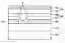
BACKGROUNDFIG. 1 is a sectional view illustrating a method of forming a metal insulating layer of a related semiconductor device and its problems.
Referring to FIG. 1, a metal interconnection layer pattern 120 exposes a part of the insulating layer 110 formed over a semiconductor substrate 100. A first metal insulating sub-layer 131 and a second metal insulating sub-layer 132 are sequentially laminated over the exposed surface of the insulating layer 110 and the metal interconnection layer pattern to form a metal insulating layer 130. The first metal insulating sub-layer 131 is formed of a high density plasma (HDP) oxide layer having a high gap filling performance. The second metal insulating sub-layer 132 is formed of a plasma enhanced-tetra ethyl ortho silicate (PE-TEOS) oxide layer. A first protective insulation sub-layer 141 for protecting a metal insulating layer and a chip and a second protective insulating sub-layer 142 are deposited over the metal insulating layer to form a protective insulating layer 140. The first protective insulating sub-layer 141 is an oxide layer and a second protective insulating sub-layer 142 is a nitride layer.
In the related method of forming the metal insulating layer, the first metal insulating sub-layer 131 is formed by repeating deposition and etching. Due to the step difference caused by the metal interconnection layer pattern 120, the top edges of the first metal insulating sub-layer 131 have sharp profiles as denoted by A in the drawing. Therefore, stress is caused by differing thermal expansion coefficients of the metal interconnection layer pattern 120 and the insulating layers in a subsequent thermal process. The stress can cause severe problems in the boundaries between the insulating layers because the top edges of the first metal insulating sub-layer 131 are sharp. As an example, when the thermally-induced stress reaches a threshold value, the top edges of the first metal insulating sub-layer 131 are cracked. In a severe example, the protective insulating layer 140 is also cracked so that the reliability of a device is significantly degraded.
SUMMARYEmbodiments relate to a method of forming a metal insulating layer of a semiconductor device, in which stress caused by the difference in the thermal expansion coefficients between a metal interconnection layer pattern and insulating layers can be attenuated, so that it is possible to prevent the insulating layers from cracking.
Embodiments relate to a method of forming a metal insulating layer of a semiconductor device. A first metal insulating sub-layer is formed over a metal interconnection layer pattern. The first metal insulating sub-layer has sharp profiles due to a step height difference in the metal interconnection layer pattern. The first metal insulating sub-layer is wet etched to round off the sharp profiles. A second metal insulating sub-layer is formed over the first metal insulating sub-layer.
The first metal insulating sub-layer may be formed of an HDP oxide layer.
The second metal insulating sub-layer may be formed of a PE-TEOS oxide layer.
A protective insulating layer including an oxide sub-layer and a nitride sub-layer may be formed over the second metal insulating sub-layer.
BRIEF DESCRIPTION OF DRAWINGSFIG. 1 is a sectional view illustrating a method of forming a metal insulating layer of a related semiconductor device and its problems;
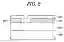
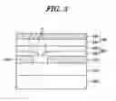
Example FIGS. 2 and 3 are sectional views illustrating a method of forming a metal insulating layer of a semiconductor device according to embodiments.
DETAILED DESCRIPTIONFIGS. 2 and 3 are sectional views illustrating a method of forming a metal insulating layer of a semiconductor device according to embodiments.
Referring to FIG. 2, an insulating layer 210 is formed over semiconductor substrate 200. A metal interconnection pattern 220 lies over and partially exposes a part of the surface of the insulating layer 210. A first metal insulating sub-layer 231 is formed over a metal interconnection layer pattern 220. Although not shown in the drawing, an active device and/or a passive device and a multi-layer metal interconnection can be aligned between the semiconductor substrate 200 and the metal interconnection layer pattern. The metal interconnection layer pattern 220 may be connected to an active and/or passive device and/or to the metal interconnection structure. The first metal insulating sub-layer 231 is formed of an HDP oxide layer. The HDP oxide layer performs well at filling gaps, however, it is very rigid, and has inferior flexibility. The first metal insulating sub-layer 231 formed of the HDP oxide layer is formed by repeated deposition and etching. The first metal insulating sub-layer 231 is deposited thicker than desired, so that it may be etched back to the desired thickness. Before etching, the top edges of the first metal insulating sub-layer 231 have sharp profiles due to the step difference caused by the metal interconnection layer pattern 220.
Referring to FIG. 3, the first metal insulating sub-layer 231 is wet etched to round off the top edges as denoted by B in the drawing. The first metal insulating sub-layer 231 was deposited with sufficient thickness so that, after wet etching, the top edges of the first metal insulating sub-layer 231 can have a rounded profile while leaving the first metal insulating sub-layer 231 with a desired thickness. Since the top edges of the first metal insulating sub-layer 231 have round profiles, stress due to differential thermal expansion between the metal interconnection layer pattern 220 and the insulating layers caused by subsequent thermal processes is released. As a result, it is possible to prevent the insulating layers from being cracked.
After the first metal insulating sub-layer 231 is etched, a second metal insulating sub-layer 232 is formed over the first metal insulating sub-layer 231 to form a metal insulating layer 230. The second metal insulating sub-layer 232 may be formed of a plasma enhanced-tetra ethyl ortho silicate (PE-TEO) oxide layer. Then, a protective insulating layer 240 is formed by depositing a first protective insulating layer 241 and a second protective insulating layer 242 over the metal insulating layer. The first protective insulating layer 241 can be formed of an oxide layer and the second protective insulating layer 242 can be formed of a nitride layer.
As described above, according to embodiments, after forming the HDP oxide layer as the first metal insulating sub-layer, the sharp edges of the HDP oxide layer are rounded off by wet etching. Therefore, stress due to the difference in the thermal expansion coefficient between the metal interconnection layer pattern and the insulating layers that can be caused by a subsequent thermal process is released. As a result, it is possible to prevent the insulating layers from being cracked.
It will be obvious and apparent to those skilled in the art that various modifications and variations can be made in the embodiments disclosed. Thus, it is intended that the disclosed embodiments cover the obvious and apparent modifications and variations, provided that they are within the scope of the appended claims and their equivalents.
Claims
What is claimed is:1. A method of forming a metal insulating layer of a semiconductor device, the method comprising:
forming a first metal insulating sub-layer over a metal interconnection layer pattern, wherein the first metal insulating sub-layer has sharp profiles due to a step height difference in the metal interconnection layer pattern;
etching the first metal insulating sub-layer to round off said sharp profiles; and
forming a second metal insulating sub-layer over the first metal insulating sub-layer.
2. The method of claim 1, wherein the first metal insulating sub-layer is wet etched.
3. The method of claim 1, wherein the first metal insulating sub-layer includes an HDP oxide layer.
4. The method of claim 1, wherein the second metal insulating sub-layer includes a PE-TEOS oxide layer.
5. The method of claim 1, further comprising:
forming a protective insulating layer over the second metal insulating sub-layer including an oxide layer and a nitride layer.
6. The method of claim 1, wherein the first metal insulating sub-layer is aligned over a metal interconnection layer which is formed over a lower insulating layer, which in turn is formed over a semiconductor substrate.
7. The method of claim 6, wherein the metal interconnection layer pattern has a gap formed therein exposing a portion of the lower insulating layer.
Images & Drawings included:
Sources:
- United States Patent and Trademark Office - verify current appl. status at the USPTO↗
Similar patent applications:
- » 20120273034
METAL SUBSTRATE WITH INSULATION LAYER AND MANUFACTURING METHOD THEREOF, SEMICONDUCTOR DEVICE AND MANUFACTURING METHOD THEREOF, SOLAR CELL AND MANUFACTURING METHOD THEREOF, ELECTRONIC CIRCUIT AND MANUFACTURING METHOD THEREOF, AND LIGHT-EMITTING ELEMENT AND MANUFACTURING METHOD THEREOF - » 20110192451
METAL SUBSTRATE WITH INSULATION LAYER AND METHOD FOR MANUFACTURING THE SAME, SEMICONDUCTOR DEVICE AND METHOD FOR MANUFACTURING THE SAME, AND SOLAR CELL AND METHOD FOR MANUFACTURING THE SAME - » 20230099330
Semiconductor device including ferroelectric layer and insulation layer with metal particles and methods of manufacturing the same - » 20150021775
Method for manufacturing semiconductor device for forming metal element-containing layer on insulating layer in which concave portion is formed, semiconductor device including insulating layer in which concave portion is formed, and semiconductor layer on insulating layer in which concave portion is formed - » 20110034028
Method for manufacturing semiconductor device having porous low dielectric constant layer formed for insulation between metal lines - » 20080318430
Method for manufacturing semiconductor device having porous low dielectric constant layer formed for insulation between metal lines - » 20230013343
Semiconductor device with interlayer insulation structure including metal-organic framework layer and method of manufacturing the same - » 20210167223
Methods for manufacturing a semiconductor device having a metal oxide layer with a concentration gradient of oxygen and an insulating layer with excess oxygen - » 20110116029
Manufacturing method for a liquid crystal display device wherein each side of a metal pattern and a semiconductor pattern facing an etched space is contacted by an insulating layer
Recent applications in this class:
- » 20250167041 2025-05-22
BEOL INTEGRATION SOLUTION BASED ON DIRECT CMP TO IMPROVE INTERMETAL DIELECTRIC LAYER - » 20250132196 2025-04-24
SEMICONDUCTOR DEVICE HAVING CAPACITOR ARRAY AND METHOD OF FORMING THE SAME - » 20250087531 2025-03-13
SEMICONDUCTOR CHIP STRUCTURE - » 20250014943 2025-01-09
Surface Profile Control Of Passivation Layers In Integrated Circuit Chips - » 20240153815 2024-05-09
SEMICONDUCTOR DEVICES AND METHOD OF MANUFACTURING THE SAME - » 20230343638 2023-10-26
SEMICONDUCTOR DEVICE STRUCTURE - » 20230121962 2023-04-20
SEMICONDUCTOR DEVICE AND METHOD FOR MANUFACTURING SAME - » 20220285208 2022-09-08
Semiconductor chip structure - » 20220157653 2022-05-19
Method for forming semiconductor device structure with source/drain contact - » 20220102201 2022-03-31
ADDITIVE DAMASCENE PROCESS
Recent applications for this Assignee:
- » 20180069111 2018-03-08
ESD protection SCR device - » 20160372592 2016-12-22
Semiconductor device and radio frequency module formed on high resistivity substrate - » 20160372483 2016-12-22
Passive device and radio frequency module formed on high resistivity substrate - » 20160062547 2016-03-03
Method of scanning touch panel and touch integrated circuit for performing the same - » 20150324031 2015-11-12
Touch Panel - » 20150270308 2015-09-24
CMOS IMAGE SENSOR AND METHOD OF MANUFACTURING THE SAME - » 20150262906 2015-09-17
COF type semiconductor package and method of manufacturing the same - » 20150122623 2015-05-07
Touch panel and method of manufacturing the same - » 20150109235 2015-04-23
Touch screen and touch panel including mutual capacitance type and self-capacitance type pixels, and driving method thereof - » 20150062998 2015-03-05
PROGRAMMABLE MEMORY