Method of substrate manufacture that decreases the package resistance
US20070148971A1
2007-06-28
11/320,273
2005-12-28
✅ Patent granted
US 7,432,202 B2
2008-10-07
-
-
S. V. Clark
2026-07-01
Abstract:
A method includes forming a coating on a land contact of a package substrate, the coating including a first material disposed between a first layer and a second layer, each of the first layer and the second layer being made of a second material including gold. An apparatus includes a package substrate including a plurality of land contacts wherein each of the plurality of land contacts includes a coating including a first material disposed between a first layer and a second layer, each of the first layer and the second layer being made of a second material including gold.
Inventors:
- Charavana K. GURUMURTHY 4 🇺🇸 Gilbert, AZ, United States
- Omar J. Bchir 3 🇺🇸 Chandler, AZ, United States
- Bijay S. SAHA 3 🇺🇸 Chandler, AZ, United States
- Munehiro TOYAMA 3 🇯🇵 Ibarakiken, Japan
- Munehiro Toyama 6 🇯🇵 Tsukubashi, Japan
- Ehab A. Nasir 1 🇺🇸 Mesa, AZ, United States
Assignee:
- INTEL CORPORATION 47,158 🇺🇸 Santa Clara, CA, United States
Interested in similar patents?
Get notified when new applications in this technology area are published.
Classification:
H01L21/44 IPC
Processes or apparatus adapted for the manufacture or treatment of semiconductor or solid state devices or of parts thereof; Manufacture or treatment of semiconductor devices or of parts thereof the devices having at least one potential-jump barrier or surface barrier, e.g. PN junction, depletion layer or carrier concentration layer the devices having semiconductor bodies not provided for in groups, , , and with or without impurities, e.g. doping materials Manufacture of electrodes on semiconductor bodies using processes or apparatus not provided for in groups -
H01L23/49811 » CPC main
Details of semiconductor or other solid state devices; Arrangements for conducting electric current to or from the solid state body in operation, e.g. leads, terminal arrangements ; Selection of materials therefor consisting of soldered constructions; Leads, on insulating substrates, Additional leads joined to the metallisation on the insulating substrate, e.g. pins, bumps, wires, flat leads
H01L23/49866 » CPC further
Details of semiconductor or other solid state devices; Arrangements for conducting electric current to or from the solid state body in operation, e.g. leads, terminal arrangements ; Selection of materials therefor consisting of soldered constructions; Leads, on insulating substrates, characterised by the materials
H05K3/244 » CPC further
Apparatus or processes for manufacturing printed circuits; Secondary treatment of printed circuits; Reinforcing the conductive pattern Finish plating of conductors, especially of copper conductors, e.g. for pads or lands
H05K3/244 » CPC further
Apparatus or processes for manufacturing printed circuits; Secondary treatment of printed circuits; Reinforcing the conductive pattern Finish plating of conductors, especially of copper conductors, e.g. for pads or lands
H01L2224/16 » CPC further
Indexing scheme for arrangements for connecting or disconnecting semiconductor or solid-state bodies and methods related thereto as covered by; Means for bonding being attached to, or being formed on, the surface to be connected, e.g. chip-to-package, die-attach, "first-level" interconnects; Manufacturing methods related thereto; Bump connectors; Manufacturing methods related thereto; Structure, shape, material or disposition of the bump connectors after the connecting process of an individual bump connector
H01L2924/01046 » CPC further
Indexing scheme for arrangements or methods for connecting or disconnecting semiconductor or solid-state bodies as covered by; Chemical elements Palladium [Pd]
H01L2924/01057 » CPC further
Indexing scheme for arrangements or methods for connecting or disconnecting semiconductor or solid-state bodies as covered by; Chemical elements Lanthanum [La]
H01L2924/01078 » CPC further
Indexing scheme for arrangements or methods for connecting or disconnecting semiconductor or solid-state bodies as covered by; Chemical elements Platinum [Pt]
H01L2924/01079 » CPC further
Indexing scheme for arrangements or methods for connecting or disconnecting semiconductor or solid-state bodies as covered by; Chemical elements Gold [Au]
H01L2924/15311 » CPC further
Indexing scheme for arrangements or methods for connecting or disconnecting semiconductor or solid-state bodies as covered by; Details of package parts other than the semiconductor or other solid state devices to be connected; Die mounting substrate; Connection portion the connection portion being formed only on the surface of the substrate opposite to the die mounting surface being a ball array, e.g. BGA
Description
FIELDIntegrated circuit packaging.
BACKGROUNDIntegrated circuits in the form of a chip or die are typically enclosed by a package that is mounted to a printed circuit board. The package has a number of external contacts on, for example, a land side of a package substrate that are connected to the printed circuit board and dedicated to the various power, ground and signal pins of the integrated circuit. Typical techniques for connecting contacts of a package with contacts of a printed circuit board include solder ball, pin, and socket techniques. In a situation where the contacts are not formed by solder balls that are attached to conductive contacts or lands of the package substrate, a typical package reference is as a land grid array (LGA) package.
A package substrate typically has internal routing layers which connect external lands to contacts on an opposite side of the substrate package that are connected to the integrated circuit chip or die. An internal routing layer typically contains separate layers for a ground bus, a power bus and a plurality of signal lines. The various layers are connected to the external lands by vias that extend through the substrate.
In general, the amount of current required of a die determines a performance of the die. If package resistance is high, current flow in the package will be reduced and the package and die will require more power. If resistance is low, the integrated circuit die can function at a lower power (e.g., 1.3 to 1.5 volts). Thus, one objective is to develop a low resistivity package.
As noted above, a package substrate has multiple conductive layers and power dissipation with respect to these layers is generally minimal. Most of the power dissipation of a substrate package occurs at the contacts or lands. Thus, in one sense, the lands determine the overall resistivity of the package substrate.
According to a current process, the external conductive lands of a package substrate are copper coated structures. For example, a copper contact formed in the substrate package is coated with a layer of nickel, followed by a coating of palladium, followed by a coating of gold.
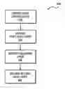
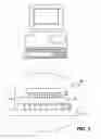
BRIEF DESCRIPTION OF THE DRAWINGSFIG. 1 shows a computer system including microprocessor enclosed by a package mounted to a printed circuit board.
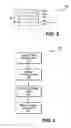
FIG. 2 shows a schematic cross-sectional side view of a land on a package substrate.
FIG. 3 shows a flow chart for forming coating layers on a land of a package substrate.
DETAILED DESCRIPTIONFIG. 1 shows a cross-sectional side view of an integrated circuit package that is physically and electrically connected to a printed wiring board or printed circuit board (PCB) to form an electronic assembly. The electronic assembly can be part of an electronic system such as a computer (e.g., desktop, laptop, handheld, server, etc.), wireless communication device (e.g., cellular phone, cordless phone, pager, etc.), computer-related peripheral (e.g., printer, scanner, monitor, etc.), entertainment device (e.g., television, radio, stereo, tapes and compact disc player, video cassette recorder, motion picture expert group audio layer 3 player (MP3), etc.), and the like. FIG. 1 illustrates the electronic assembly as part of a desktop computer. FIG. 1 shows electronic assembly 100 including die 110, physically and electrically connected to package substrate 120. Die 110 is an integrated circuit die, such as a microprocessor die, having, for example, transistor structures interconnected or connected to power/ground or input/output signals external to the die through interconnect lines to contacts 130 on an external surface of die 110. Contacts 130 may be aligned with contacts 140 making up, for example, a die bump layer on an external surface of package substrate 120. On a surface of package substrate 120 opposite a surface including contacts 140 are land contacts 150. Connected to each of land contacts 150 are solder bumps 160 that may be used to connect package 170 to circuit board 180, such as a motherboard or other circuit board.
FIG. 2 shows an example of one of the land contacts of the package substrate of FIG. 1. FIG. 3 describes a representative process flow for forming coating layers on a contact. Referring to FIG. 2, package substrate 120 includes land contacts 150 each of which includes contact 210 formed in or on package substrate 120 as a contact point. Contact 210 has a number of coating layers overlying a surface (a top surface as viewed). In one embodiment, contact 210 is an electrically conductive material such as copper or an alloy of copper. Contact 210 may be separated by adjacent contacts on package substrate 120 through a dielectric material, such as a polymer (e.g., polyimide) material.
Overlying a surface of contact 210 (a top surface as viewed) is first coating layer 220. In an embodiment where contact 210 is a copper material, first coating layer 220 is a nickel material formed. Referring to the process flow in FIG. 3, process 300 includes depositing a first coating layer such as a nickel material on a land contact of a package substrate, such as land contact 210 of package substrate 120 (block 310). One technique for depositing a first coating layer of a nickel material onto a contact of a copper material is through an electroless deposition process.
Overlying first coating layer 220 in the structure of FIG. 2 is layer 230. Layer 230 is selected, in one embodiment, of a material of gold. The process flow described in FIG. 3 includes depositing a first gold layer on the first coating layer (block 320). One technique for depositing a gold material is through an electroplating process.
Overlying layer 230 in the structure shown in FIG. 2 is layer 240 of, in one embodiment, a palladium material. Process 300 of FIG. 3 includes depositing palladium layer on first gold layer (block 330). In one embodiment, palladium is deposited through an electroplating process.
The depositing of palladium is followed by a deposition of a second gold layer (block 340, FIG. 3). In one embodiment, the second gold layer is deposited by an electroplating process. FIG. 2 shows overlying layer 250 of a material of gold overlying layer 240. Thus, the structure shown in FIG. 2 includes layer 240 sandwiched or disposed between layer 230 and layer 250 of a material of gold.
In one embodiment, a coating of nickel (Ni)/gold (Au)/palladium (Pd) is deposited to the following thicknesses: Ni 5.6 microns; Au 0.025 micron; Pd 0.08 micron; Au 0.06 micron. A total thickness of the composite coating in this example, is 5.75 microns. If this composite coating is compared to a prior art coating utilizing 5.6 microns nickel, 0.8 microns palladium, and 0.6 micron gold for a composite thickness of 5.73 microns, a prediction on a resistance of the composite stacks would be the stack with the additional gold layer would have a higher resistance as a thicker stack. However, although an overall resistance might be predicted to be higher, it has been found that an electronic structure (e.g., a work function) of the metal is such that tunneling of electrons through the composite stack is easier when the palladium material is sandwiched between gold layers as described.
In the preceding detailed description, reference is made to specific embodiments thereof. It will, however, be evident that various modifications and changes may be made thereto without departing from the broader spirit and scope of the following claims. The specification and drawings are, accordingly, to be regarded in an illustrative rather than a restrictive sense.
Claims
1. A method comprising:
forming a coating on a land contact of a package substrate configured to connect to a circuit die, the coating comprising a first material disposed between a first layer and a second layer, each of the first layer and the second layer being made of a second material comprising gold.
2. The method of claim 1, wherein the first material comprises palladium.
3. A method comprising:
forming a first coating on a land contact of a package substrate; and
forming a second coating on the land contact comprising a first material disposed between a first layer and a second layer, each of the first layer and the second layer being made of a second material comprising gold.
4. The method of claim 3, wherein the first coating comprises nickel.
5. The method of claim 1, wherein the first material comprises palladium and the coating is a second coating, the method further comprising:
prior to forming the second coating, forming a first coating comprising nickel.
6. The method of claim 1, wherein forming a coating comprises electrodepositing the first layer and the second layer.
7. The method of claim 6, wherein electrodepositing comprising electroplating.
8. An apparatus comprising:
a package substrate configured to connect to a circuit die, the package substrate comprising a plurality of land contacts wherein each of the plurality of land contacts comprises a coating comprising a first material disposed between a first layer and a second layer, each of the first layer and the second layer being made of a second material comprising gold.
9. The apparatus of claim 8, wherein the coating is a second coating, the package substrate further comprising a first coating on each of the plurality of contacts, the first coating disposed between the second coating and the land contact.
10. The apparatus of claim 9, wherein the first coating comprises nickel.
11. The apparatus of claim 8, wherein the first material comprises palladium.
12. The apparatus of claim 8, wherein the plurality of contacts comprise a first plurality of contacts on a first side of the package substrate, the package substrate further comprises a plurality of second contacts on a second opposite side of the package substrate, the apparatus further comprising:
a chip coupled to the plurality of second contacts.
13. A system comprising:
a computing device comprising:
a microprocessor;
a printed circuit board; and
a substrate, wherein the microprocessor is coupled to the printed circuit board through the substrate, the substrate comprising a plurality of land contacts wherein each of the plurality of land contacts comprises a coating comprising a first material disposed between a first layer and a second layer, each of the first layer and the second layer being made of a second material comprising gold.
14. The system of claim 13, wherein the coating is a second coating, the package substrate further comprising a first coating on each of the plurality of contacts, the first coating disposed between the second coating and the land contact.
15. The system of claim 9, wherein the first coating comprises nickel.
16. The system of claim 15, wherein the first material comprises palladium.
Images & Drawings included:
Sources:
- United States Patent and Trademark Office - verify current appl. status at the USPTO↗
Recent applications in this class:
- » 20250293129 2025-09-18
SUBSTRATE UNIT - » 20250285950 2025-09-11
SEMICONDUCTOR DEVICE PACKAGE - » 20250273548 2025-08-28
PACKAGE COMPRISING A BRIDGE WITH SPRING PADS - » 20250253220 2025-08-07
POWER SEMICONDUCTOR MODULE ARRANGEMENT - » 20250253219 2025-08-07
PRESS-FIT TERMINAL AND SEMICONDUCTOR DEVICE - » 20250253218 2025-08-07
SEMICONDUCTOR PACKAGE AND MANUFACTURING METHOD OF SEMICONDUCTOR PACKAGE - » 20250253217 2025-08-07
PACKAGE COMPRISING SUBSTRATES WITH POST INTERCONNECTS - » 20250246526 2025-07-31
SEMICONDUCTOR MODULE - » 20250226299 2025-07-10
SEMICONDUCTOR PACKAGE AND METHOD FOR FABRICATING THE SAME - » 20250218912 2025-07-03
POLYMER HYBRID BONDING FOR COMPOSITE PACKAGES AND METHODS OF FORMING THE SAME
Recent applications for this Assignee:
- » 20250294866 2025-09-18
GATE CUT CONFINED WITHIN GATE TRENCH - » 20250294846 2025-09-18
BACKSIDE CROSS-COUPLE INTERCONNECTS - » 20250294835 2025-09-18
ELONGATED VERTICAL STRUCTURES OF CHANNEL MATERIALS - » 20250294827 2025-09-18
CO-INTEGRATION OF GATE-ALL-AROUND DEVICES WITH DIFFERENT NUMBERS OF NANORIBBONS - » 20250294818 2025-09-18
TRANSISTOR DESIGNS FOR FLOATING BODY MEMORY - » 20250294781 2025-09-18
MAGNETIC CORE INDUCTORS ON PACKAGE SUBSTRATES - » 20250294777 2025-09-18
INTEGRATED CIRCUIT DEVICE WITH MEMORY ARRAY AND SHARED GAIN ELEMENT - » 20250293985 2025-09-18
RECEIVER-BASED PRECISION CONGESTION CONTROL - » 20250293860 2025-09-18
PRESERVATION OF CONFIDENTIALITY AND INTEGRITY OF MODELS DURING EXECUTION - » 20250293706 2025-09-18
LOW-RANK DECOMPOSITION-BASED HARDWARE COMPRESSION OF MATRICES AND TENSORS