Gate structure in a trench region of a semiconductor device and method for manufacturing the same
US20070152245A1
2007-07-05
11/646,837
2006-12-27
✅ Patent granted
US 7,541,641 B2
2009-06-02
-
-
Ida M Soward
2026-12-31
Abstract:
Disclosed is a semiconductor device. The semiconductor device includes; a pair of drift regions formed in a semiconductor substrate; a trench region formed between the pair of drift regions; an oxide layer spacer on both sidewalls of the trench region; a gate formed in the trench region; and a source and a drain formed in the pair of the drift regions, respectively.
Assignee:
- Dongbu Electronics Co., Ltd. 766 🇰🇷 Seoul, South Korea
Interested in similar patents?
Get notified when new applications in this technology area are published.
Classification:
H01L29/76 IPC
Semiconductor devices adapted for rectifying, amplifying, oscillating or switching, or capacitors or resistors with at least one potential-jump barrier or surface barrier, e.g. PN junction depletion layer or carrier concentration layer; Details of semiconductor bodies or of electrodes thereof; Multistep manufacturing processes therefor; Types of semiconductor device ; Multistep manufacturing processes therefor controllable by only the electric current supplied, or only the electric potential applied, to an electrode which does not carry the current to be rectified, amplified or switched Unipolar devices, e.g. field effect transistors
H01L29/94 IPC
Semiconductor devices adapted for rectifying, amplifying, oscillating or switching, or capacitors or resistors with at least one potential-jump barrier or surface barrier, e.g. PN junction depletion layer or carrier concentration layer; Details of semiconductor bodies or of electrodes thereof; Multistep manufacturing processes therefor; Types of semiconductor device ; Multistep manufacturing processes therefor controllable only by variation of the electric current supplied, or only the electric potential applied, to one or more of the electrodes carrying the current to be rectified, amplified, oscillated or switched; Capacitors with potential-jump barrier or surface barrier Metal-insulator-semiconductors, e.g. MOS
H01L31/062 IPC
Semiconductor devices sensitive to infra-red radiation, light, electromagnetic radiation of shorter wavelength or corpuscular radiation and specially adapted either for the conversion of the energy of such radiation into electrical energy or for the control of electrical energy by such radiation; Processes or apparatus specially adapted for the manufacture or treatment thereof or of parts thereof; Details thereof adapted as photovoltaic [PV] conversion devices characterised by at least one potential-jump barrier or surface barrier the potential barriers being only of the metal-insulator-semiconductor type
H01L31/113 IPC
Semiconductor devices sensitive to infra-red radiation, light, electromagnetic radiation of shorter wavelength or corpuscular radiation and specially adapted either for the conversion of the energy of such radiation into electrical energy or for the control of electrical energy by such radiation; Processes or apparatus specially adapted for the manufacture or treatment thereof or of parts thereof; Details thereof in which radiation controls flow of current through the device, e.g. photoresistors characterised by at least one potential-jump barrier or surface barrier, e.g. phototransistors; Devices sensitive to infra-red, visible or ultra-violet radiation characterised by field-effect operation, e.g. junction field-effect phototransistor being of the conductor-insulator-semiconductor type, e.g. metal-insulator-semiconductor field-effect transistor
H01L31/119 IPC
Semiconductor devices sensitive to infra-red radiation, light, electromagnetic radiation of shorter wavelength or corpuscular radiation and specially adapted either for the conversion of the energy of such radiation into electrical energy or for the control of electrical energy by such radiation; Processes or apparatus specially adapted for the manufacture or treatment thereof or of parts thereof; Details thereof in which radiation controls flow of current through the device, e.g. photoresistors characterised by at least one potential-jump barrier or surface barrier, e.g. phototransistors; Devices sensitive to very short wavelength, e.g. X-rays, gamma-rays or corpuscular radiation characterised by field-effect operation, e.g. MIS type detectors
Description
BACKGROUND OF THE INVENTION1. Field of the Invention
The present invention relates to a semiconductor device and a method for manufacturing the same.
2. Description of the Related Art
High voltage devices require a low-density drift region in a drain so as to have breakdown characteristics against high voltages. The drift region occupies the largest area in the high voltage device. Larger drift region is required in a horizontal direction as the higher breakdown characteristic is required for the high voltage device.
Further, in order to realize a high voltage breakdown characteristic, it is necessary for the high voltage device to increase the length of a channel region for preventing the punch through between a source and a drain. The channel region occupies the second largest area in the high voltage device.
Hereinafter, a high voltage device according to the related art will be described in detail with reference to the attached drawings.
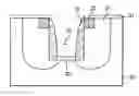
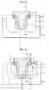
FIG. 1 is a cross-sectional view of a high voltage device according to the related art.
Referring to FIG. 1, a low-density drift region 11 is formed on a predetermined region of a p-type semiconductor substrate 10. A gate oxide layer 12 is formed on an upper surface of the p-type semiconductor substrate 10, and a field oxide layer 13 for a field plate is formed on the semiconductor substrate 10 corresponding to a part of the drift region 11.
A gate 14 is formed on the gate oxide layer 12 and the field plate 13. A source 15 and a drain 16, i.e., n-type doped region 15 having a high-density are formed adjacent to both sides of the gate 14 and in the semiconductor substrate 10. At this time, the source 15 is spaced apart from the drift region 11, and the drain 16 is formed in the drift region 11.
The channel region 17 is formed between the source 15 and the drift region 11 in the semiconductor substrate 10 below the gate 14, and electrons 18 flow from the source region 15 to the drain region 16.
In the conventional high voltage device as described above, the drift region 11 needs to be increased in its horizontal length due to its horizontal structure so as to improve the breakdown characteristic. This may act as limitations in high-integration and miniaturization of the semiconductor device.
SUMMARY OF THE INVENTIONAccordingly, the present invention has been made to solve the above-mentioned problems, and an object of the present invention is to provide a semiconductor device and a method for manufacturing the same, which can reduce an area of a device while sustaining the breakdown strength.
To accomplish the above object of the present invention, there is provided a semiconductor device, which comprises a pair of drift regions formed in a semiconductor substrate; a trench region formed between the pair of drift regions; an oxide layer spacer formed on both sidewalls of the trench region; an insulating layer formed below the trench region; a gate formed in the trench region; and a source and a drain formed in the pair of the drift regions, respectively.
To accomplish the above object of the present invention, there is provided a method for manufacturing a semiconductor device, which comprises the steps of: forming a pair of drift regions in a semiconductor substrate; forming an oxide layer on the substrate in such a manner that the oxide layer is partially overlapped with the pair of drift regions; forming a trench region between the pair of drift regions; forming an oxide layer spacer on both sidewalls of the trench region; forming an insulating layer below the trench region; forming a gate in the trench region and on the oxide layer; and forming a source and a drain on the pair of drift regions, respectively.
BRIEF DESCRIPTION OF THE DRAWINGSFIG. 1 is a cross-sectional view of a high voltage device according to the related art; and
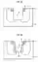
FIGS. 2A to 2G are cross-sectional views showing a semiconductor device and a method for manufacturing the same according to a preferred embodiment of the present invention.
DETAILED DESCRIPTION OF THE INVENTIONHereinafter, a preferred embodiment according to the present invention will be described in detail, with reference to the following drawings.
In the following description of the present invention, technologies which are generally known in the art and do not directly relate to the present invention will be omitted in order to avoid redundancy and to clarify the subject manner of the present invention. In the same manner, some of elements are exaggerated, omitted or simplified in the drawings and the elements may have sizes different from those shown in drawings, in practice.
FIG. 2A to 2G are cross-sectional views showing a semiconductor device and a method for manufacturing the same according to a preferred embodiment of the present invention.
First, as shown in FIG. 2A, a pair of drift regions 21, which are symmetrical to each other, are formed in a p-type semiconductor substrate 20.
The drift regions 21 are deeply formed in the vertical direction, and spaced apart from each other in the horizontal direction by a predetermined distance.
A method for forming the drift region 21 includes the steps of; forming a drift region mask pattern in the semiconductor substrate 20; implanting n-type low-density impurities; and driving-in the implanted impurities.
Next, as shown in FIG. 2B, an oxide layer 22 is formed on the surface of the substrate 20 such that the oxide layer 22 is partially overlapped with both drift regions 21. In other words, the length of the oxide layer 22 is larger than the distance between both drift regions 21.
A method for forming the oxide layer 22 includes the steps of; forming an oxide layer mask pattern on the substrate 20; etching the substrate 20 by a predetermined depth; depositing the oxide layer 22 over the entire surface; and planarizing the oxide layer 22.
As shown in 2C, a nitride layer 31 is formed on the substrate 20.
Next, as shown in 2D, a trench region 23 is formed between both drift regions and in the substrate 20.
The trench region 23 has a depth than equal to or shallower than that of the drift region 21, and a width shorter than the length of the oxide layer 22.
A method for forming the trench region 23 includes the steps of; forming a trench region mask pattern; and etching the substrate 20 by a predetermined depth.
Next, as shown in FIG. 2E, an oxide layer spacer 24 is formed on both sidewalls of the trench region 23. The oxide layer spacer 24 is used as a field plate of a high voltage device. A method for forming the oxide layer spacer 24 includes the steps of; depositing the oxide layer over the entire surface; and anisotropic dry etching the deposited oxide layer.
An insulating layer 32 is formed below the trench region 23. The insulating layer 32 is a thermal oxide layer formed by performing a thermal oxidation process.
Next, the nitride layer 31 is removed.
Next, as shown in FIG. 2F, a gate 25 is formed in the trench region 23 and on the upper surface of the oxide layer 22. After that, a nitride layer spacer 26 is formed on both sidewalls of the gate 25.
A method for forming the gate 25 includes the steps of; depositing a gate conductive layer so as to be completely filled in the trench region 23; forming a gate mask pattern; and etching the gate conductive layer. Further, a method for forming the nitride layer spacer 26 includes the steps of; depositing the nitride layer over the entire surface; and anisotropic dry etching the deposited nitride layer.
Next, as shown in FIG. 2G, a source 27 and a drain 28 are formed on both drift regions 21, respectively, by implanting n-type impurities having a high density.
Further, electrons 30 flow between the source 27 and the drain 28.
As described above, the semiconductor device is featured in that the drift regions 21 having a vertical structure are formed to be symmetrical to each other in the left and right direction.
In the high voltage device according to the present invention, since a depletion region is formed in a vertical direction when a high electric power is applied to the drain 28, both lengths of the drift region 21 and the channel region 29 can be shorter about a several μm than that of the conventional structure, thereby reducing the area of the high voltage device.
While the present invention has been described with reference to the particular illustrative embodiments, it is not to be restricted by the embodiments but only by the appended claims. It is to be appreciated that those skilled in the art can change or modify the embodiments without departing from the scope and spirit of the present invention.
Claims
What is claimed is:1. A semiconductor device comprising:
first and second drift regions in a semiconductor substrate;
a trench region between the first and second drift regions;
an oxide layer spacer on sidewalls of the trench region;
an insulating layer below the trench region;
a gate in the trench region; and
a source in one of the first and second drift regions and a drain in the other of the first and second drift regions.
2. The semiconductor device according to claim 1, wherein the trench region has a depth that is equal to or less than that of the first and second drift regions.
3. The semiconductor device according to claim 1, wherein the gate includes a spacer on sidewalls thereof.
4. The semiconductor device according to claim 3, wherein the spacer comprises silicon nitride.
5. The semiconductor device according to claim 1, wherein the first and second drift regions are spaced apart from each other in a horizontal direction.
6. The semiconductor device according to claim 1, wherein the first and second drift regions each have a depth that is greater than a width thereof.
7. The semiconductor device according to claim 1, further comprising an oxide layer adjacent to the trench region.
8. The semiconductor device according to claim 8, wherein a part of the gate is on the upper surface of the oxide layer.
9. A method for manufacturing a semiconductor device, the method comprising the steps of:
forming first and second drift regions in a semiconductor substrate;
forming an oxide layer on the substrate such that the oxide layer partially overlaps the first and second drift regions;
forming a trench between the first and second drift regions;
forming an oxide spacer on sidewalls of the trench;
forming an insulating layer at a bottom of the trench;
forming a gate in the trench and on the oxide layer; and
forming a source in one of the first and second drift regions and a drain in the other of the first and second drift regions.
10. The method according to claim 9, wherein the step of forming the oxide layer includes:
forming a mask pattern on the substrate;
etching the substrate to a predetermined depth;
depositing the oxide layer over an entire surface of the semiconductor substrate; and
planarizing the oxide layer.
11. The method according to claim 9, wherein the trench has a depth equal to or less than that of the first and second drift regions and a width equal to or less than a length of the oxide layer.
12. The method according to claim 11, wherein the width of the trench is less than the length of the oxide layer.
13. The method according to claim 9, further comprising forming a spacer on sidewalls of the gate.
14. The method according to claim 13, wherein the spacer comprises silicon nitride.
15. The method according to claim 9, wherein the first and second drift regions are symmetrical to and spaced apart from each other in a horizontal direction.
16. A method for manufacturing a semiconductor device, the method comprising the steps of:
forming first and second drift regions in a semiconductor substrate;
forming an oxide layer on the substrate such that the oxide layer overlaps with each of the first and second drift regions;
forming a nitride layer on the substrate;
forming a trench between the first and second drift regions;
forming an oxide spacer on sidewalls of the trench;
forming an insulating layer at a bottom of the trench;
removing the nitride layer;
forming a gate in the trench region and at least partially on the oxide layer; and
forming a source in one of the first and second drift regions and a drain in the other of the first and second drift regions.
17. The method according to claim 16, wherein the trench has a depth less than that of the first and second drift regions and a width less than a length of the oxide layer.
18. The method according to claim 16, further comprising forming a nitride spacer on sidewalls of the gate.
Images & Drawings included:
Sources:
- United States Patent and Trademark Office - verify current appl. status at the USPTO↗
Similar patent applications:
- » 20090209073
Gate structure in a trench region of a semiconductor device and method for manufacturing the same - » 20210408279
Semiconductor device including trench gate structure and buried shielding region and method of manufacturing - » 20240222498
Semiconductor device including trench gate structure and buried shielding region and method of manufacturing - » 20250234588
SEMICONDUCTOR DEVICE INCLUDING TRENCH GATE STRUCTURE AND BURIED SHIELDING REGION AND METHOD OF MANUFACTURING - » 20210167203
Method of manufacturing a silicon carbide semiconductor device with trench gate structure and vertical pn junction between body region and drift structure
Recent applications in this class:
- » 20220344495 2022-10-27
FIN STRUCTURES HAVING VARIED FIN HEIGHTS FOR SEMICONDUCTOR DEVICE - » 20210376124 2021-12-02
Radical Etching in Gate Formation - » 20200152773 2020-05-14
Fin structures having varied fin heights for semiconductor device - » 20200105908 2020-04-02
Radical etching in gate formation - » 20190123169 2019-04-25
Electronic device including transistor and method for fabricating the same - » 20190088765 2019-03-21
COMPOUND SEMICONDUCTOR FIELD EFFECT TRANSISTOR WITH SELF-ALIGNED GATE - » 20190067451 2019-02-28
Fin structures having varied fin heights for semiconductor device - » 20190067450 2019-02-28
Fin structures having varied fin heights for semiconductor device - » 20190027582 2019-01-24
Integrated circuit devices with blocking layers - » 20180277657 2018-09-27
Compound semiconductor field effect transistor with self-aligned gate
Recent applications for this Assignee:
- » 20100314675 2010-12-16
Power semiconductor device and method for manufacturing the same - » 20100133421 2010-06-03
Complementary metal oxide silicon image sensor and method of fabricating the same - » 20100029051 2010-02-04
Semiconductor device and fabricating method thereof - » 20100019353 2010-01-28
Semiconductor device and method for manufacturing the same - » 20090317953 2009-12-24
Memory device and method for manufacturing the same - » 20090317952 2009-12-24
Memory device and method for manufacturing the same - » 20090317949 2009-12-24
ESD protecting circuit and manufacturing method thereof - » 20090302361 2009-12-10
Complementary metal oxide semiconductor (CMOS) image sensor - » 20090278205 2009-11-12
High voltage BICMOS device and method for manufacturing the same - » 20090273032 2009-11-05
LDMOS device and method for manufacturing the same