Transistor device and method for manufacturing the same
US20070152284A1
2007-07-05
11/615,804
2006-12-22
✅ Patent granted
US 7,427,546 B2
2008-09-23
-
-
Minh-Loan Tran | Selim Ahmed
2026-12-26
Abstract:
A transistor device includes a recess in a surface of semiconductor substrate, a gate insulation layer formed over an inner side of the recess, a gate conductor filling the recess in which the gate insulation layer is formed, and source and drain regions located over the substrate adjacent the recess. Among the advantages: the gate structure lowers overall gate resistance and reduces the short channel effect.
Assignee:
- Dongbu HiTek Co., Ltd. 896 🇰🇷 Seoul, South Korea
Interested in similar patents?
Get notified when new applications in this technology area are published.
Classification:
H01L29/76 IPC
Semiconductor devices adapted for rectifying, amplifying, oscillating or switching, or capacitors or resistors with at least one potential-jump barrier or surface barrier, e.g. PN junction depletion layer or carrier concentration layer; Details of semiconductor bodies or of electrodes thereof; Multistep manufacturing processes therefor; Types of semiconductor device ; Multistep manufacturing processes therefor controllable by only the electric current supplied, or only the electric potential applied, to an electrode which does not carry the current to be rectified, amplified or switched Unipolar devices, e.g. field effect transistors
H01L21/3205 IPC
Processes or apparatus adapted for the manufacture or treatment of semiconductor or solid state devices or of parts thereof; Manufacture or treatment of semiconductor devices or of parts thereof the devices having at least one potential-jump barrier or surface barrier, e.g. PN junction, depletion layer or carrier concentration layer the devices having semiconductor bodies comprising elements of Group IV of the Periodic System or AB compounds with or without impurities, e.g. doping materials; Treatment of semiconductor bodies using processes or apparatus not provided for in groups - to form insulating layers thereon, e.g. for masking or by using photolithographic techniques ; After treatment of these layers; Selection of materials for these layers Deposition of non-insulating-, e.g. conductive- or resistive-, layers on insulating layers; After-treatment of these layers
Description
The present application claims priority under 35 U.S.C. 119 and 35 U.S.C. 365 to Korean Patent Application No. 10-2005-0133428 (filed on Dec. 29, 2005), which is hereby incorporated by reference in its entirety.
BACKGROUND
When a transistor of a semiconductor device is formed, a structure of a gate may soar relatively high over a silicon substrate. This may create problems in defining the length of the gate when the devices are scaled down. Also, when lightly doped drain ion implants and source and drain ion implants are formed, masking steps are required. Thus the cost for fabricating the devices is increased.
Therefore, there has been a need to create a transistor device having a new gate structure.
SUMMARY
Embodiments relate to semiconductor device, and more particularly, to a method for fabricating a transistor that may overcome a short channel effect (SCE).
Accordingly, embodiments are directed to a transistor device and a method for manufacturing the same that substantially obviates one or more problems due to limitations and disadvantages of the related art.
Embodiments relate to a transistor device and a method for manufacturing the same, which effectively may reduce size of a semiconductor device.
Additional advantages, objects, and features of the embodiments will be set forth in part in the description which follows and in part will become apparent to those having ordinary skill in the art upon examination of the following or may be learned from practice of the embodiments. The objectives and other advantages of the embodiments may be realized and attained by the structure particularly pointed out in the written description and claims hereof as well as the appended drawings.
Embodiments relate to a method for fabricating a transistor by forming a first insulation layer and a second insulation layer over a semiconductor substrate; selectively etching the first and second insulation layers and semiconductor substrate to form a recess; depositing a gate insulation layer and a gate conductor layer; planarizing the gate insulation layer and the gate conductor layer to form a gate structure filling the recess; removing the second insulation layer; forming a spacer over a side wall of the gate; implanting ions into the semiconductor substrate near the spacer to form source and drain regions; wet etching the second insulation layer and the gate insulation layer to expose an upper side wall of the gate and upper portions of the source and drain regions; and forming a salicide layer on the exposed surface of the gate and over the source and drain regions.
The planarizing may be carried out by chemical mechanical polishing (CMP) of the gate conductor using the second insulation layer as a polishing stop layer.
The LDD and the source and drain ion implantation profile may be formed by ion implantation using a mask once in the source and drain regions. The gate conductor may include polysilicon, and the gate insulation layer may include nitride-based oxide, hafnium-based oxide, tantalum-based oxide, or titanium-based oxide.
The recess may be etched to a depth of 500 Å to 2000 Å.
The wet etching of the second insulation layer leaves a portion of the second insulation layer which is over the source and drain regions, adjacent the gate insulation layer and below the spacer. The spacer entirely covers and extends beyond the top surface of the second insulation layer.
Embodiments relate to a transistor device including a recess in a surface of semiconductor substrate; a gate insulation layer formed over an inner side of the recess; a gate conductor filling the recess in which the gate insulation layer is formed; and source and drain regions located over the substrate adjacent the recess. An upper portion of the gate conductor projects above the surface of the semiconductor substrate. A spacer may be formed over the side wall of a gate insulation portion that is projected above the surface of semiconductor substrate. A salicide layer may be formed over a upper portion of the gate and over the source and drain regions.
Embodiments relate to a transistor device and a method for manufacturing the same, which effectively may reduce size of a semiconductor device.
It is to be understood that both the foregoing general description and the following detailed description of the embodiments are exemplary and explanatory and are intended to provide further explanation of the claimed subject matter.
BRIEF DESCRIPTION OF THE DRAWINGS
FIGS. 1 through 7 are sectional views illustrating a transistor device and a method for fabricating the same according to embodiments.
DETAILED DESCRIPTION
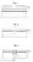
With reference to FIG. 1, a first insulation layer 3 and a second insulation layer 5 are deposited over a semiconductor substrate 1. A first photoresist mask layer 100 is formed over the insulating layers for etching the first insulation layer 3 and the second insulation layer 5. First insulation layer 3 may be composed of silicon oxide while the second insulation layer 5 may be composed of silicon nitride.
In FIG. 2, the first and the second insulation layer 3 and 5 are selectively etched using mask 100 to create patterns 3′ and 5′, which collectively constitute etching mask 6. A dry etching process using mask 6 forms recess 2 in the semiconductor substrate 1. The recess 2 may be etched to a depth of approximately 500 Å to 2000 Å.
In FIG. 3, a gate insulation layer 7 and a gate conductor layer are deposited. A gate 9 and the gate insulation layer 7 are planarized using a chemical mechanical polishing (CMP) method using the pattern of the second insulation layer 5′ as a stop layer. Therefore, gate 9, which fills recess 2, is approximately 500 Å to 2000 Å thick. The gate 9 may include polysilicon and the gate insulation layer may include a nitride-based oxide, hafnium-based oxide, tantalum-based oxide, or titanium-based oxide.
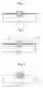
In FIG. 4, the pattern of the insulation layer 5′ has been completely removed using, for example, a wet etching method using phosphoric acid solution.
With reference to FIG. 5, after depositing a layer for the spacer 11 over the side wall of the gate 7, spacer 11 is formed by using for example, a front etching method. The spacer 11 may also be formed by an isotropic etching method. And then LDD and high density source and drain regions 13′ are formed by implanting ions. The ion implantation process is performed once at the LDD and source and drain regions 13′ to form a profile of the LDD and source/drain regions 13′. The ion implant profile after annealing is shown.
In FIG. 6, a gate insulation layer 7′ and a second pattern 3″ of the first insulation layer are formed by wet etching. The second pattern 3″ of the first insulation layer forms a recessed filler over the gate insulation layer 7′ between the spacer 11 and LDD region. Gate insulation 7′ is recessed from the top plane of the gate and spacers 11, to expose an upper side wall of the gate 9.
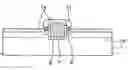
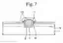
In FIG. 7, a salicide process is performed on gate 9, and source and drain regions 13 to form salicide layer 15. The salicide layer 15 is formed by heat treatment between 700 to 1000° C., after depositing one of, for example, cobalt, nickel, and Ti over the whole surface.
As described, embodiments relate to a method for fabricating a semiconductor transistor. A new scheme, facilitating a scaling down of the size of the transistors, is proposed. The gate resistance may be reduced without increasing the area used on the surface of the substrate. Lateral diffusion of the ion implant source may be more easily controlled to reduce the short channel effect. It is therefore possible to implement a shallow well ion implantation process at a smaller device scale, with smaller transistor features.
It will be obvious and apparent to those skilled in the art that various modifications and variations can be made in the embodiments disclosed. Thus, it is intended that the disclosed embodiments cover the obvious and apparent modifications and variations, provided that they are within the scope of the appended claims and their equivalents.
Claims
What is claimed is:1. A method for fabricating a transistor comprising:
forming a first insulation layer and a second insulation layer over a semiconductor substrate;
selectively etching the first and second insulation layers and semiconductor substrate to form a recess;
depositing a gate insulation layer and a gate conductor layer;
planarizing the gate insulation layer and the gate conductor layer to form a gate structure filling the recess;
removing the second insulation layer;
forming a spacer over a side wall of the gate;
implanting ions into the semiconductor substrate near the spacer to form source and drain regions;
wet etching the second insulation layer and the gate insulation layer to expose an upper side wall of the gate and upper portions of the source and drain regions; and
forming a salicide layer on the exposed surface of the gate and over the source and drain regions.
2. A method according to claim 1, wherein the planarizing comprises chemical mechanical polishing (CMP) of the gate conductor using the second insulation layer as a polishing stop layer.
3. A method according to claim 1, wherein the LDD and the source and drain ion implantation profile is formed by ion implantation using a mask once in the source and drain regions.
4. A method according to claim 1, wherein the gate conductor includes polysilicon.
5. A method according to claim 1, wherein the gate insulation layer includes one selected from the group consisting of nitride-based oxide, hafnium-based oxide, tantalum-based oxide, and titanium-based oxide.
6. A method according to claim 1, wherein the recess is etched to a depth of 500 Å to 2000 Å.
7. A method according to claim 1, wherein said wet etching the second insulation layer leaves a portion of the second insulation layer which is over the source and drain regions, adjacent the gate insulation layer and below the spacer.
8. A method according to claim 7, wherein said the spacer entirely covers and extends beyond a top surface of said portion of the second insulation layer.
9. A transistor device comprising:
a semiconductor substrate having a recess;
a gate insulation layer covering the bottom and sides of the recess;
a gate conductor filling the recess and projected over the semiconductor substrate;
a spacer over the upper sidewall of the gate;
source and drain regions formed over the semiconductor substrate near the spacer; and
a salicide layer formed over the gate, and the source and drain regions.
10. A transistor device comprising:
a recess in a surface of semiconductor substrate;
a gate insulation layer formed over an inner side of the recess;
a gate conductor filling the recess in which the gate insulation layer is formed; and
source and drain regions located over the substrate adjacent the recess.
11. A transistor device according to claim 10, wherein an upper portion of the gate conductor projects above the surface of the semiconductor substrate.
12. A transistor device according to claim 11, wherein a spacer is formed over the side wall of a gate insulation portion that is projected above the surface of semiconductor substrate.
13. A transistor device according to claim 10, wherein a salicide layer is formed over a upper portion of the gate and over the source and drain regions.
14. A transistor device according to claim 10, wherein the gate region is made of polysilicon.
15. A method according to claim 10, wherein the gate insulation layer includes one selected from the group consisting of nitride-based oxide, hafnium-based oxide, tantalum-based oxide, and titanium-based oxide.
Images & Drawings included:
Sources:
- United States Patent and Trademark Office - verify current appl. status at the USPTO↗
Similar patent applications:
- » 20120211758
Thin-film transistor device manufacturing method, thin-film transistor device, and display device - » 20130164892
Thin-film transistor device manufacturing method, thin-film transistor device, and display device - » 20120286282
Thin-film transistor device manufacturing method, thin-film transistor device, and display device - » 20120206668
Thin-film transistor device manufacturing method, thin-film transistor, and display device - » 20200098902
Insulated gate bipolar transistor device, manufacturing method for semiconductor device, and manufacturing method for insulated gate bipolar transistor device - » 20110220896
Transistor, display device, electronic device, manufacturing method of transistor, and manufacturing method of display device - » 20080017931
Metal-oxide-semiconductor transistor device, manufacturing method thereof, and method of improving drain current thereof - » 20160336359
Thin film transistor device, manufacturing method thereof, and display apparatus - » 20080194070
Metal-oxide-semiconductor transistor device, manufacturing method thereof, and method of improving drain current thereof - » 20170365720
Transistor, electronic device, manufacturing method of transistor
Recent applications in this class:
- » 20200395466 2020-12-17
Transistor comprising a lengthened gate - » 20190296129 2019-09-26
Method and structure of forming finFET contact - » 20190252520 2019-08-15
LONG CHANNELS FOR TRANSISTORS - » 20190214482 2019-07-11
Transistors with H-shaped or U-shaped channels and method for forming the same - » 20190214481 2019-07-11
Method and structure of forming FinFET contact - » 20190189776 2019-06-20
Long channels for transistors - » 20190027581 2019-01-24
Transistor comprising a lengthened gate - » 20170047426 2017-02-16
Complementary metal oxide semiconductor field effect transistor, metal oxide semiconductor field effect transistor and manufacturing method thereof - » 20160329412 2016-11-10
MOS transistor and fabrication method - » 20160247897 2016-08-25
Drain extended MOS transistors with split channel
Recent applications for this Assignee:
- » 20180069111 2018-03-08
ESD protection SCR device - » 20160372592 2016-12-22
Semiconductor device and radio frequency module formed on high resistivity substrate - » 20160372483 2016-12-22
Passive device and radio frequency module formed on high resistivity substrate - » 20160062547 2016-03-03
Method of scanning touch panel and touch integrated circuit for performing the same - » 20150324031 2015-11-12
Touch Panel - » 20150270308 2015-09-24
CMOS IMAGE SENSOR AND METHOD OF MANUFACTURING THE SAME - » 20150262906 2015-09-17
COF type semiconductor package and method of manufacturing the same - » 20150122623 2015-05-07
Touch panel and method of manufacturing the same - » 20150109235 2015-04-23
Touch screen and touch panel including mutual capacitance type and self-capacitance type pixels, and driving method thereof - » 20150062998 2015-03-05
PROGRAMMABLE MEMORY