Optical module
US20070154150A1
2007-07-05
11/546,258
2006-10-12
✅ Patent granted
US 7,364,371 B2
2008-04-29
-
-
Frank G. Font | Ryan Lepisto
2026-10-12
Abstract:
An optical module has plural optical units each having an optical communication device that performs conversion between an electrical signal and an optical signal, and a socket that the optical communication device is fitted in. The optical units are aligned and detachably connected to each other by a part of the socket in contact with the socket of the adjacent optical unit.
Assignee:
- FUJI XEROX CO., LTD. 11,478 🇯🇵 Tokyo, Japan
Interested in similar patents?
Get notified when new applications in this technology area are published.
Classification:
H01L29/22 IPC
Semiconductor devices adapted for rectifying, amplifying, oscillating or switching, or capacitors or resistors with at least one potential-jump barrier or surface barrier, e.g. PN junction depletion layer or carrier concentration layer; Details of semiconductor bodies or of electrodes thereof; Multistep manufacturing processes therefor; Semiconductor bodies ; Multistep manufacturing processes therefor characterised by the materials of which they are formed including, apart from doping materials or other impurities, only AB compounds
G02B6/42 » CPC main
Light guides; Coupling light guides Coupling light guides with opto-electronic elements
G02B6/4284 » CPC further
Light guides; Coupling light guides; Coupling light guides with opto-electronic elements; Packages, e.g. shape, construction, internal or external details; Electrical aspects of optical modules with disconnectable electrical connectors
G02B6/36 IPC
Light guides; Coupling light guides Mechanical coupling means
H01L29/205 IPC
Semiconductor devices adapted for rectifying, amplifying, oscillating or switching, or capacitors or resistors with at least one potential-jump barrier or surface barrier, e.g. PN junction depletion layer or carrier concentration layer; Details of semiconductor bodies or of electrodes thereof; Multistep manufacturing processes therefor; Semiconductor bodies ; Multistep manufacturing processes therefor characterised by the materials of which they are formed including, apart from doping materials or other impurities, only AB compounds including two or more compounds, e.g. alloys in different semiconductor regions, e.g. heterojunctions
H01L33/00 IPC
Semiconductor devices with at least one potential-jump barrier or surface barrier specially adapted for light emission; Processes or apparatus specially adapted for the manufacture or treatment thereof or of parts thereof; Details thereof
Description
BACKGROUND
(i) Technical Field
The present invention relates to an optical module that has an optical communication device and a socket that the optical communication device is fitted in.
(ii) Related Art
In recent years, optical communication has been performed using optical fibers and an optical communication device that includes a head performing conversion between an electrical signal and an optical signal, and a metallic lead extending from the head and transmitting an electrical signal.
SUMMARY
According to an aspect of the present invention, an optical module has plural optical units each having an optical communication device that performs conversion between an electrical signal and an optical signal, and a socket that the optical communication device is fitted in,
the optical units being aligned and detachably connected to each other by a portion of the socket in contact with the socket of the adjacent optical unit.
BRIEF DESCRIPTION OF THE DRAWINGS
Exemplary embodiment(s) of the present invention will be described in detail based on the following figures, wherein:
FIG. 1 shows an external perspective view of an optical module according to one exemplary embodiment of the invention;
FIG. 2 shows an external perspective view of the optical module shown in FIG. 1 as viewed from its back;
FIG. 3 shows a sectional view of an optical unit constituting part of the optical module according to the exemplary embodiment; and
FIG. 4 shows the state where adjacent optical units are detachably connected.
DETAILED DESCRIPTION
The exemplary embodiment of the invention will be described below with reference to the accompanying drawings.
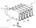
FIG. 1 shows an external perspective view of an optical module 1 according to the exemplary embodiment of the invention.
The optical module 1 of FIG. 1 is composed of five optical units 10 detachably arranged in order. Each of five optical units 10 has an optical communication device 11, however, the optical communication devices of the optical units 10 other than the leftmost are omitted in FIG. 1 for the sake of convenience.
The optical unit 10 is composed of an optical communication device 11 and a socket 12 with openings 12a (see FIG. 3) that receive the optical communication device 11. The optical communication device 11 is composed of a head 110 that performs conversion between an electrical signal and an optical signal, and two leads 111 that extend from the head 110 and transmits an electrical signal. FIG. 1 also shows an electrode 121 connected to one of the two leads 111.
Interference prevention walls 123 are disposed between adjacent sockets 12. Each of the interference prevention walls 123 extends to the front side of the optical module 1 and in parallel to an optical axis of the optical communication device 11 so as to prevent interference in an optical signal by the optical communication device 11 of its adjacent optical unit(s) 10.
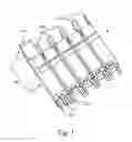
FIG. 2 shows an external perspective view of the optical module 1 as viewed from its back.
FIG. 2 shows the other electrode 122 connected to the other lead 111 (also see FIG. 3).
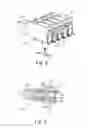
FIG. 3 shows a sectional view of the optical unit 10 constituting part of the optical module 1 according to the exemplary embodiment.
FIG. 3 shows the state where the leads 111 are fitted in the openings 12a formed in the socket 12 of the optical unit 10. As shown in FIG. 3, the leads 111 each have a rectangular portion between the ends thereof.
FIG. 3 also shows that the leads 111 fitted in the openings 12a are respectively in contact with the electrodes 121 and 122 that are attached to the socket 12.
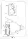
Part (a) and part (b) of FIG. 4 show the state where adjacent optical units are detachably connected. Part (b) of FIG. 4 shows the remaining part of the optical unit 10 that is not shown in part (a) of FIG. 4. In part (b) of FIG. 4, an adjacent optical unit is not indicated for the sake of convenience.
Referring to part (a) of FIG. 4, a portion 123a of the interference prevention wall 123 of the socket 12 is connected to the adjacent socket 12. As shown in part (b) of FIG. 4, a convex portion 124 formed at the bottom of a flank of the socket 12 and an end portion 1211 of the electrode 121 are detachably attached thereto and used for connection with the adjacent socket 12.
According to the exemplary embodiment, if, for example, an optical module of four optical units is required, one out of the five optical units 10 is to be detached. At that time, force is applied at first to the portion 123a of the interference prevention wall 123 disposed in the front side of the optical unit 10, to separate the portion 123a from its adjacent optical unit 12. Then, the convex portion 124 and the end portion 1211 of the electrode 121 are cut off.
In the above-described embodiment, five optical units 10 are detachably aligned, however, the present invention is not limited thereto and may have another number of optical units. Or, the interference prevention wall 123 may not be provided in the optical module 1. Such modification does not substantially deteriorate the effect of the invention. Additionally, the portion to be connected may be other than the portion 123a of the interference prevention wall 123, the convex portion 124 formed at the bottom of the flank of the socket 12 and the end portion 1211 of the electrode 121, as long as part of adjacent sockets are connected to each other.
The foregoing description of the exemplary embodiment(s) of the present invention has been provided for the purposes of illustration and description. It is not intended to be exhaustive or to limit the invention to the precise forms disclosed. Obviously, many modifications and variations will be apparent to practitioners skilled in the art. The exemplary embodiments were chosen and described in order to best explain the principles of the invention and its practical applications, thereby enabling other skilled in the art to understand the invention for various embodiments and with the various modifications as are suited to the particular use contemplated. It is intended that the scope of the invention be defined by the following claims and their equivalents.
Claims
What is claimed is:1. An optical module comprising:
a plurality of optical units each having an optical communication device that performs conversion between an electrical signal and an optical signal and a socket that the optical communication device is fitted in,
the optical units being aligned and detachably connected to each other by a portion of the socket in contact with the socket of the adjacent optical unit.
2. The optical module according to claim 1, wherein the socket has an interference prevention wall that extends toward the front of the optical module in the direction parallel to an optical axis of an optical signal operated by the optical communication device, and prevents interference in the optical signal operated by the optical communication device of the adjacent optical unit.
3. The optical module according to claim 1, wherein the optical communication device includes a head that performs conversion between an electrical signal and an optical signal, and two metallic leads that extend from the head and transmits the electrical signal,
the optical unit has an electrode that is attached to the socket and is in contact with one of the two leads, and
a plurality of the electrodes are aligned corresponding to the aligned optical units and the adjacent electrodes are partially and detachably connected to each other.
Images & Drawings included:
Sources:
- United States Patent and Trademark Office - verify current appl. status at the USPTO↗
Similar patent applications:
- » 10050865
OPTICAL MODULATOR, OPTICAL MODULATOR MANUFACTURING METHOD, LIGHT INFORMATION PROCESSING APPARATUS INCLUDING OPTICAL MODULATOR, IMAGE FORMATION APPARATUS INCLUDING OPTICAL MODULATOR, AND IMAGE PROJECTION AND DISPLAY APPARATUS INCLUDING OPTICAL MODULATOR - » 20050264866
Optical modulator, optical modulator manufacturing method, light information processing apparatus including optical modulator, image formation apparatus including optical modulator, and image projection and display apparatus including optical modulator - » 20250264746
OPTICAL MODULATION DEVICE, OPTICAL MODULATOR, OPTICAL MODULATION MODULE, OPTICAL TRANSMISSION APPARATUS, AND OPTICAL TRANSMISSION SYSTEM - » 20250264745
OPTICAL MODULATION DEVICE, OPTICAL MODULATOR, OPTICAL MODULATION MODULE, OPTICAL TRANSMISSION APPARATUS, AND OPTICAL TRANSMISSION SYSTEM - » 20250264744
OPTICAL MODULATION DEVICE, OPTICAL MODULATOR, OPTICAL MODULATION MODULE, OPTICAL TRANSMISSION APPARATUS, AND OPTICAL TRANSMISSION SYSTEM - » 20170242316
Optical modulator element, optical modulation module including optical modulator element, and method for manufacturing optical modulator element - » 20170192177
Optical module, optical module mounting method, optical module-mounted circuit substrate, optical module evaluation kit system, circuit substrate, and communication system - » 20160116695
Optical module, optical module mounting method, optical module-mounted circuit substrate, optical module evaluation kit system, circuit substrate, and communication system - » 20220381977
Optical waveguide device, manufacturing method of optical modulation element, optical modulator, optical modulation module, and optical transmission apparatus - » 20200110291
Optical modulator, substrate for optical modulator, method of manufacturing optical modulator, and method of manufacturing substrate for optical modulator
Recent applications in this class:
- » 20250138256 2025-05-01
OPTICAL APPARATUS, LIGHT EMITTING APPARATUS, OPTICAL CABLE, AND METHOD OF CONNECTING OPTICAL APPARATUS - » 20250020873 2025-01-16
HYBRID MANUFACTURING FOR INTEGRATING PHOTONIC AND ELECTRONIC COMPONENTS - » 20240411090 2024-12-12
METHOD OF FORMING PHOTONICS STRUCTURES - » 20240176081 2024-05-30
Vertical Integrated Photonics Chiplet for In-Package Optical Interconnect - » 20240094481 2024-03-21
Optical apparatus, light emitting apparatus, optical cable, and method of connecting optical apparatus - » 20230035957 2023-02-02
Light source device - » 20230026564 2023-01-26
Optoelectronic transmitter with phased array antenna comprising an integrated control device - » 20220214508 2022-07-07
Optical module - » 20210011231 2021-01-14
Photodetector structure - » 20210003792 2021-01-07
Light receiving device, and light transmitting and receiving device
Recent applications for this Assignee:
- » 20220100142 2022-03-31
Protection member, replacement component with protection member, and image forming apparatus - » 20220091549 2022-03-24
Light-emitting-device head and image forming apparatus with switching unit defining switching positions coinciding with dots in an image - » 20220091542 2022-03-24
Particle conveying device and image forming apparatus - » 20220091532 2022-03-24
IMAGE FORMING APPARATUS AND LIGHT-EMITTING-DEVICE HEAD - » 20220091529 2022-03-24
Toner for developing electrostatic charge image, electrostatic charge image developer, toner cartridge, process cartridge, image forming apparatus, and image forming method - » 20220091528 2022-03-24
Toner for electrostatic image development, electrostatic image developer, and toner cartridge - » 20220091527 2022-03-24
Electrostatic image developing toner, electrostatic image developer, and toner cartridge - » 20220091526 2022-03-24
Toner for developing electrostatic charge image, electrostatic charge image developer, toner cartridge, process cartridge, image forming apparatus, and image forming method - » 20220091525 2022-03-24
Toner for developing electrostatic charge image, electrostatic charge image developer, toner cartridge, process cartridge, image forming apparatus, and image forming method - » 20220091524 2022-03-24
Electrostatic image developing toner, electrostatic image developer, toner cartridge, process cartridge, image forming apparatus, and image forming method