Method of fabricating a semiconductor device having a pre metal dielectric liner
US20070155111A1
2007-07-05
11/615,750
2006-12-22
✅ Patent granted
US 7,645,705 B2
2010-01-12
-
-
Dung A. Le
2028-01-17
Abstract:
A method of fabricating a semiconductor device including forming a pre metal dielectric liner over a semiconductor substrate on which a transistor is formed. The pre metal dielectric liner is sputter etched to form an unstable interface at the surface. The boron is trapped in an interface in an unstable state in a surface of the PMD liner to effectively suppress the boron penetration phenomenon to the semiconductor substrate.
Assignee:
- Dongbu HiTek Co., Ltd. 896 🇰🇷 Seoul, South Korea
Interested in similar patents?
Get notified when new applications in this technology area are published.
Classification:
H01L21/76825 » CPC further
Processes or apparatus adapted for the manufacture or treatment of semiconductor or solid state devices or of parts thereof; Manufacture or treatment of devices consisting of a plurality of solid state components formed in or on a common substrate or of parts thereof; Manufacture of integrated circuit devices or of parts thereof; Manufacture of specific parts of devices defined in group; Applying interconnections to be used for carrying current between separate components within a device comprising conductors and dielectrics characterised by the formation and the after-treatment of the dielectrics, e.g. smoothing; Modification of the material of dielectric layers, e.g. grading, after-treatment to improve the stability of the layers, to increase their density etc. by exposing the layer to particle radiation, e.g. ion implantation, irradiation with UV light or electrons etc.
H01L21/76829 » CPC further
Processes or apparatus adapted for the manufacture or treatment of semiconductor or solid state devices or of parts thereof; Manufacture or treatment of devices consisting of a plurality of solid state components formed in or on a common substrate or of parts thereof; Manufacture of integrated circuit devices or of parts thereof; Manufacture of specific parts of devices defined in group; Applying interconnections to be used for carrying current between separate components within a device comprising conductors and dielectrics characterised by the formation and the after-treatment of the dielectrics, e.g. smoothing characterised by the formation of thin functional dielectric layers, e.g. dielectric etch-stop, barrier, capping or liner layers
H01L21/8222 IPC
Processes or apparatus adapted for the manufacture or treatment of semiconductor or solid state devices or of parts thereof; Manufacture or treatment of devices consisting of a plurality of solid state components formed in or on a common substrate or of parts thereof; Manufacture of integrated circuit devices or of parts thereof; Manufacture or treatment of devices consisting of a plurality of solid state components or integrated circuits formed in, or on, a common substrate with subsequent division of the substrate into plural individual devices to produce devices, e.g. integrated circuits, each consisting of a plurality of components the substrate being a semiconductor, using silicon technology Bipolar technology
H01L21/302 IPC
Processes or apparatus adapted for the manufacture or treatment of semiconductor or solid state devices or of parts thereof; Manufacture or treatment of semiconductor devices or of parts thereof the devices having at least one potential-jump barrier or surface barrier, e.g. PN junction, depletion layer or carrier concentration layer the devices having semiconductor bodies comprising elements of Group IV of the Periodic System or AB compounds with or without impurities, e.g. doping materials; Treatment of semiconductor bodies using processes or apparatus not provided for in groups - to change their surface-physical characteristics or shape, e.g. etching, polishing, cutting
Description
The present application claims priority under 35 U.S.C. 119 and 35 U.S.C. 365 to Korean Patent Application No. 10-2005-0134173 (filed on Dec. 29, 2005), which is hereby incorporated by reference in its entirety.
BACKGROUND
In general, when forming a Complementary Metal Oxide Semiconductor (CMOS) in which an n channel type MOS transistor and a p channel MOS transistor are integrated on the same substrate, gate patterns and a silicide are formed. Then, to fill a space between the gate patterns, an insulating layer is formed using a Boron Phospho Silicate Glass (BPSG) oxide layer, having excellent flowability.
To suppress the diffusion of boron B in the BPSG oxide layer into a substrate during a subsequent thermal process, a pre metal dielectric (PMD) liner is formed prior to a deposition of the BPSG oxide layer.
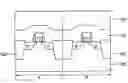
FIG. 1 is a cross-sectional view showing a semiconductor device having a general pre metal dielectric liner.
With reference to FIG. 1, a device isolation layer 102 defines an active region of a semiconductor substrate 100 having first region A and second region B.
An n-channel type transistor is arranged in the first region A of the semiconductor device 100, and a p-channel type transistor is arranged in the second region B of the semiconductor device 100.
Further, a nitride layer 110 is arranged over an entire surface of the substrate as the PMD liner, and the BPSG oxide layer 120 is formed over the nitride layer 110.
The nitride layer 110 serves as an etch stop layer during a subsequent etching for a contact. Simultaneously, nitride layer 110 functions to suppress the diffusion of boron B in the BPSG oxide layer 120 into the semiconductor substrate 100 during a subsequent thermal treatment. When an impurity ion such as the boron B penetrates the semiconductor substrate 100, the threshold voltage of a device is locally changed, which degrades the stability of the device. In the related art, in order to suppress the penetration of the boron B to the highest degree, a gas atmosphere is controlled to increase the bonding strength of nitrogen-hydrogen N—H during the formation of the nitride layer 110. However, using only the method according to the related art, the suppression of boron B penetration into the semiconductor substrate 100 is limited. Moreover, it requires a thick nitride layer 110 as the PMD liner.
SUMMARY
Accordingly, embodiments relate to a method of fabricating a semiconductor device having a pre metal dielectric liner that substantially obviates one or more problems due to limitations and disadvantages of the related art.
Embodiments relate to a method of fabricating a semiconductor device having a pre metal dielectric liner, which may improve the reliability of a device by suppressing a penetration of boron in a BPSG used as an insulating layer into a semiconductor substrate to the highest degree.
Additional advantages, objects, and features of the embodiments will be set forth in part in the description which follows and in part will become apparent to those having ordinary skill in the art upon examination of the following or may be learned from practical experience with the embodiments. The objectives and other advantages of the embodiments may be realized and attained by the structure particularly pointed out in the written description and claims hereof as well as the appended drawings.
To achieve these objects and other advantages and in accordance with the purpose of the embodiments, there is provided a method of fabricating a semiconductor device including forming a pre metal dielectric liner over a semiconductor substrate on which a transistor is formed. The pre metal dielectric liner is sputter etched to form an unstable interface at the surface.
A BPSG oxide layer may be formed over the pre metal dielectric liner. The pre metal dielectric liner may be formed of a nitride layer. The sputtering-etching for the pre metal dielectric liner may be performed using argon ions.
It is to be understood that both the foregoing general description and the following detailed description of the embodiments are exemplary and explanatory and are intended to provide further explanation of the claims.
BRIEF DESCRIPTION OF THE DRAWINGS
FIG. 1 is a cross-sectional view showing a semiconductor device having a pre metal dielectric liner;
Example FIGS. 2 to 4 are a cross-sectional view showing a method for manufacturing a semiconductor device having a pre metal dielectric liner according to embodiments; and
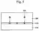
FIG. 5 is a view for illustrating a boron diffusion suppression effect of a semiconductor device having a pre metal dielectric liner formed by the method according to embodiments.
DETAILED DESCRIPTION
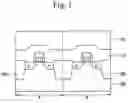
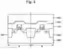
FIGS. 2 to 4 are a cross-sectional view showing a method for manufacturing a semiconductor device having a pre metal dielectric liner according to embodiments.
First, referring to FIG. 2, a device isolation layer 202 is formed in semiconductor substrate 200 having a first region A and a second region B to define an active region. Although the device isolation layer 202 is a trench device isolation layer, embodiments are not limited thereto. Next, an n-channel type MOS transistor and a p channel type MOS transistor are formed in the first region A and the second region B to constitute a complementary MOS (CMOS) transistor. In the embodiment, the embodiment has been described that the CMOS transistor is formed on the semiconductor substrate 200. However, the CMOS transistor is integrated in the semiconductor substrate 200 together with an active device and a passive device. Otherwise, one of the active device and the passive device can be integrated in the semiconductor substrate 200.
N+ type source/drain regions are formed in the first region A of the semiconductor substrate 200 in which an n-channel type MOS transistor is formed, and a gate insulating layer is interposed above a channel region therebetween to support a gate conductive layer. A metal silicide layer is arranged over the gate conductive layer. A gate spacer layer is arranged over the sides of the gate conductive layer and the metal silicide layer. Although not shown in the drawings, a metal silicide layer can be arranged over upper portions of the source/drain regions. P+ type source/drain regions are arranged in the second region B of the semiconductor substrate 200 in which the p-channel type MOS transistor is formed, and a gate insulating layer is interposed above a channel region therebetween to support a gate conductive layer. A metal silicide layer is arranged over the gate conductive layer. A gate spacer layer is arranged over the sides of the gate conductive layer and the metal silicide layer. Although not shown in the drawings, a metal silicide layer can be arranged over upper portions of the source/drain regions. As described above, after the n-channel type MOS transistor and the p-channel type MOS transistor have been formed, a nitride layer 210 is formed over an entire surface thereof as a pre metal dielectric liner.
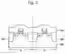
With reference to FIG. 3, as illustrated in the drawing by arrows, an argon sputtering etching process is performed over the surface of the nitride layer 210. In the sputtering etching process, an argon ion collides with the nitride layer 210 surface to form an interface 210′ (of FIG. 4) in an unstable energy state. To change the unstable state to a stable state, the interface 210′ (of FIG. 4) has an affinity for impurities and ions. It functions as a trap with respect to penetrating ions.
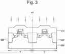
With reference to FIG. 4, after argon sputtering etching has formed an interface 210′ with an unstable energy state at the surface, a BPSG oxide layer 220 is formed over the nitride layer 210.
FIG. 5 is a view for illustrating a boron permeation suppression effect of a semiconductor device having a pre metal dielectric liner formed by the method according to embodiments.
With reference to FIG. 5, the interface 210′ having an unstable energy state at the surface is present on the surface of a nitride layer 210, and a BPSG oxide layer 220 is formed over the nitride layer 210.
When a subsequent thermal treatment is carried out, boron B ions 222 in the BPSG oxide layer 220 become exited and move towards the semiconductor substrate. The interface 210′ present at a surface of the nitride layer 210 traps the boron B ions 222 before they penetrate the semiconductor substrate. The trapped ions change an unstable state to a stable state. Accordingly, the boron B ions are trapped in the interface 210′ of the nitride layer 210 and he penetrating phenomenon is suppressed.
As is understood from the forgoing description, in a method of fabricating a semiconductor device having a pre metal dielectric liner, after the PMD has formed an interface at the surface of the PMD liner, the sputtering etching process is performed. Accordingly, the boron B is trapped in an interface in an unstable state in a surface of the PMD liner to effectively suppress the boron penetration phenomenon in the semiconductor substrate.
It will be obvious and apparent to those skilled in the art that various modifications and variations can be made in the embodiments disclosed. Thus, it is intended that the disclosed embodiments cover the obvious and apparent modifications and variations, provided that they are within the scope of the appended claims and their equivalents.
Claims
What is claimed is:1. A method of fabricating a semiconductor device comprising:
forming a pre metal dielectric liner over an entire surface of a semiconductor substrate on which a transistor is formed;
sputtering-etching the pre metal dielectric liner to form an unstable interface at a surface thereof; and
forming a BPSG oxide layer over the pre metal dielectric liner.
2. The method according to claim 1, wherein the pre metal dielectric liner is formed of a nitride layer.
3. The method according to claim 1, wherein, the sputtering-etching for the pre metal dielectric liner is performed using argon ions.
4. A method of fabricating a semiconductor device comprising:
forming a pre metal dielectric liner over an entire surface of a semiconductor substrate on which a transistor is formed;
sputtering-etching the pre metal dielectric liner to form an unstable interface at a surface thereof; and
forming a BPSG oxide layer over the sputtering-etched pre metal dielectric liner.
5. The method according to claim 4, wherein a sputtering-etching for the pre metal dielectric liner uses argon ions.
Images & Drawings included:
Sources:
- United States Patent and Trademark Office - verify current appl. status at the USPTO↗
Recent applications in this class:
- » 20230335445 2023-10-19
HYBRID BIOFILM SEMICONDUCTOR INFORMATION SYSTEMS - » 20220359294 2022-11-10
Method of making 3D segmented devices for enhanced 3D circuit density - » 20190279906 2019-09-12
Semiconductor device and method for manufacturing the same - » 20180350690 2018-12-06
Multiplexer and integrated circuit using the same - » 20180144985 2018-05-24
CMOS process-dependent near-threshold voltage regulation - » 20150357243 2015-12-10
Method for making strained semiconductor device and related methods - » 20150214112 2015-07-30
Semiconductor device and method for forming the same - » 20150108576 2015-04-23
Method for fabricating NMOS and PMOS transistors on a substrate of the SOI, in particular FDSOI, type and corresponding integrated circuit - » 20150079740 2015-03-19
Method for fabricating semiconductor device having an embedded source/drain - » 20150069517 2015-03-12
Complementary metal oxide semiconductor device and method of manufacturing the same
Recent applications for this Assignee:
- » 20180069111 2018-03-08
ESD protection SCR device - » 20160372592 2016-12-22
Semiconductor device and radio frequency module formed on high resistivity substrate - » 20160372483 2016-12-22
Passive device and radio frequency module formed on high resistivity substrate - » 20160062547 2016-03-03
Method of scanning touch panel and touch integrated circuit for performing the same - » 20150324031 2015-11-12
Touch Panel - » 20150270308 2015-09-24
CMOS IMAGE SENSOR AND METHOD OF MANUFACTURING THE SAME - » 20150262906 2015-09-17
COF type semiconductor package and method of manufacturing the same - » 20150122623 2015-05-07
Touch panel and method of manufacturing the same - » 20150109235 2015-04-23
Touch screen and touch panel including mutual capacitance type and self-capacitance type pixels, and driving method thereof - » 20150062998 2015-03-05
PROGRAMMABLE MEMORY