Method for forming a dual interlayer dielectric layer of a semiconductor device
US20070155162A1
2007-07-05
11/644,890
2006-12-26
✅ Patent granted
US 7,645,697 B2
2010-01-12
-
-
Thao Le
2028-04-02
Abstract:
A method for forming a dual interlayer dielectric layer, which is capable of preventing an interlayer delamination phenomenon generated between an etch stop layer and an interlayer dielectric layer is provided. An interlayer dielectric layer of a dual structure is formed such that a first interlayer dielectric layer and a second interlayer dielectric layer are sequentially stacked on the etch stop layer. The etch stop layer is formed on a substrate, the substrate having a source/drain region and a gate formed therein. The dual interlayer dielectric layer is selectively etched, and a conductive material is deposited thereon, thereby forming a contact. The O3-TEOS layer and the PE-TEOS layer used as the first interlayer dielectric layer can relieve a compressive stress and improve adhesion force, respectively, thereby preventing the interlayer delamination phenomenon.
Assignee:
- Dongbu Electronics Co., Ltd. 766 🇰🇷 Seoul, South Korea
Interested in similar patents?
Get notified when new applications in this technology area are published.
Classification:
H01L21/76837 » CPC main
Processes or apparatus adapted for the manufacture or treatment of semiconductor or solid state devices or of parts thereof; Manufacture or treatment of devices consisting of a plurality of solid state components formed in or on a common substrate or of parts thereof; Manufacture of integrated circuit devices or of parts thereof; Manufacture of specific parts of devices defined in group; Applying interconnections to be used for carrying current between separate components within a device comprising conductors and dielectrics characterised by the formation and the after-treatment of the dielectrics, e.g. smoothing Filling up the space between adjacent conductive structures; Gap-filling properties of dielectrics
C23C16/402 » CPC further
Chemical coating by decomposition of gaseous compounds, without leaving reaction products of surface material in the coating, i.e. chemical vapour deposition [CVD] processes characterised by the deposition of inorganic material, other than metallic material; Deposition of compounds, mixtures or solid solutions, e.g. borides, carbides, nitrides; Oxides containing silicon Silicon dioxide
C23C16/505 » CPC further
Chemical coating by decomposition of gaseous compounds, without leaving reaction products of surface material in the coating, i.e. chemical vapour deposition [CVD] processes characterised by the method of coating using electric discharges using radio frequency discharges
H01L21/022 » CPC further
Processes or apparatus adapted for the manufacture or treatment of semiconductor or solid state devices or of parts thereof; Manufacture or treatment of semiconductor devices or of parts thereof; Forming layers; Forming insulating materials on a substrate characterised by the type of layer, e.g. type of material, porous/non-porous, pre-cursors, mixtures or laminates the layer being a laminate, i.e. composed of sublayers, e.g. stacks of alternating high-k metal oxides
H01L21/02304 » CPC further
Processes or apparatus adapted for the manufacture or treatment of semiconductor or solid state devices or of parts thereof; Manufacture or treatment of semiconductor devices or of parts thereof; Forming layers; Forming insulating materials on a substrate characterised by the treatment performed before or after the formation of the layer pre-treatment formation of intermediate layers, e.g. buffer layers, layers to improve adhesion, lattice match or diffusion barriers
H01L21/76801 » CPC further
Processes or apparatus adapted for the manufacture or treatment of semiconductor or solid state devices or of parts thereof; Manufacture or treatment of devices consisting of a plurality of solid state components formed in or on a common substrate or of parts thereof; Manufacture of integrated circuit devices or of parts thereof; Manufacture of specific parts of devices defined in group; Applying interconnections to be used for carrying current between separate components within a device comprising conductors and dielectrics characterised by the formation and the after-treatment of the dielectrics, e.g. smoothing
H01L21/76829 » CPC further
Processes or apparatus adapted for the manufacture or treatment of semiconductor or solid state devices or of parts thereof; Manufacture or treatment of devices consisting of a plurality of solid state components formed in or on a common substrate or of parts thereof; Manufacture of integrated circuit devices or of parts thereof; Manufacture of specific parts of devices defined in group; Applying interconnections to be used for carrying current between separate components within a device comprising conductors and dielectrics characterised by the formation and the after-treatment of the dielectrics, e.g. smoothing characterised by the formation of thin functional dielectric layers, e.g. dielectric etch-stop, barrier, capping or liner layers
H01L21/4763 IPC
Processes or apparatus adapted for the manufacture or treatment of semiconductor or solid state devices or of parts thereof; Manufacture or treatment of semiconductor devices or of parts thereof the devices having at least one potential-jump barrier or surface barrier, e.g. PN junction, depletion layer or carrier concentration layer the devices having semiconductor bodies not provided for in groups, , , and with or without impurities, e.g. doping materials; Treatment of semiconductor bodies using processes or apparatus not provided for in groups to change their surface-physical characteristics or shape, e.g. etching, polishing, cutting Deposition of non-insulating, e.g. conductive -, resistive -, layers on insulating layers; After-treatment of these layers
Description
RELATED APPLICATION
This application is based upon and claims the benefit of priority to Korean Application No. 10-2005-0134182 filed on Dec. 29, 2005, the entire contents of which are incorporated herein by reference.
BACKGROUND
1. Technical Field
The present invention relates to a method for manufacturing a semiconductor device. More specifically, the present invention relates to a method for forming a dual interlayer dielectric layer capable of preventing an interlayer delamination phenomenon generated between an etch stop layer and an interlayer dielectric layer.
2. Description of the Related Art
As the current trend in semiconductor devices change toward high integration and smaller sizes, a borderless contact (BLC) technique has been suggested in order to assure a margin capable of compensating for a misalignment in a contact process. Such a technique refers to a method in which a contact is self-aligned by means of a sidewall spacer of a gate when the contact is formed inside the interlayer dielectric layer (ILD) so as to connect with a source/drain region of a silicon substrate. Thus, the borderless contact technique is referred to as a self-aligned contact (SAC) method.
However, such a contact may partially overlap an isolation layer due to mask misalignment. Therefore, the borderless contact technique typically requires an etch stop layer in order to protect an isolation layer in an anisotropic plasma etching process forming a contact hole. This is because the isolation layer may be physically damaged by the contact hole etching process which causes a leakage current, thereby deteriorating the qualities of the semiconductor device.
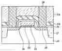
FIG. 1 is a cross-sectional view showing a structure of an interlayer dielectric layer of a semiconductor device according to the related art.
As shown in FIG. 1, a gate insulating layer 12 and a gate 13 are formed on a silicon substrate 10 including an isolation layer 11. A sidewall spacer 14 is formed on both sidewalls of gate 13, respectively, and a source/drain region 15 is formed in silicon substrate 10. A silicide (not shown) is formed on source/drain region 15 and gate 13, respectively. Etch stop layer 16 is formed in such a manner as to cover the entire structure, and an interlayer dielectric layer 17 is sequentially formed on etch stop layer 16. A contact hole is formed by etching interlayer dielectric layer 17, and then a conductive material (e.g., tungsten) is deposited in the contact hole, thereby forming a contact 18.
In such a conventional structure, etch stop layer 16 is made of silicon nitride, and interlayer dielectric layer 17 includes an oxide layer formed using high-density plasma chemical vapor deposition (hereinafter, refers to as a “HDP-CVD”) having superior gap fill capacity. However, an interlayer delamination phenomenon is frequently generated since the adhesion force between etch stop layer 16 and interlayer dielectric layer 17 is weak. Further, compressive stress of etch stop layer 16 and interlayer dielectric layer 17 stacked on etch stop layer 16 accumulates, causing the interlayer delamination phenomenon. When such interlayer delamination phenomenon is generated, the contact material penetrates into the etched region during the subsequent process, i.e., a contact material deposition process, causing an electric short and deteriorating the product yield of the semiconductor device.
BRIEF SUMMARY
To solve the above-mentioned problems occurring in the prior art, there is provided consistent with the present invention an interlayer dielectric layer structure and a method for forming the same, which is capable of improving an adhering capacity between an etch stop layer and an interlayer dielectric layer, as well as attenuating stress therebetween.
Consistent with the present invention there is also provided an interlayer dielectric layer structure and a method for forming the same, which is capable of preventing an interlayer delamination phenomenon generated between an etch stop layer and an interlayer dielectric layer during a contact material deposition process.
Consistent with the present invention, there is further provided a method for forming a dual interlayer dielectric layer of a semiconductor device having a structure, which will be described below.
A method for forming a dual interlayer dielectric layer consistent with the present invention comprises: forming an etch stop layer on a substrate, the substrate having a source/drain region and a gate formed therein; depositing a first interlayer dielectric layer including O3-TEOS on the etch stop layer; flattening the first interlayer dielectric layer; depositing a second interlayer dielectric layer including PE-TEOS on the first interlayer dielectric layer; and forming a contact by selectively etching the first interlayer dielectric layer and the second interlayer dielectric layer and depositing a conductive material thereon.
Further, another method for forming a dual interlayer dielectric layer consistent with the present invention comprises: forming an etch stop layer on a substrate, the substrate having a source/drain region and a gate formed therein; depositing a first interlayer dielectric layer formed of PE-TEOS on the etch stop layer; depositing a second interlayer dielectric layer formed of HDP-CVD on the first interlayer dielectric layer; and forming a contact by selectively etching the first interlayer dielectric layer and the second interlayer dielectric layer and depositing a conductive material thereon.
In a method for forming the dual interlayer dielectric layer consistent with the present invention, the etch stop layer may be made of a silicon nitride. Further, the first interlayer dielectric layer and the second interlayer dielectric layer have preferable deposition conditions, respectively.
Meanwhile, consistent with the present invention there is also provided a dual interlayer dielectric layer of the semiconductor device formed by the method as described above.
BRIEF DESCRIPTION OF THE DRAWINGS
FIG. 1 is a cross-sectional view showing a structure of an interlayer dielectric layer of a semiconductor device according to the conventional invention.
FIG. 2 is a cross-sectional view showing a structure of a dual interlayer dielectric layer of a semiconductor device according to a preferred embodiment consistent with the present invention.
FIG. 3 is a cross-sectional view showing a structure of a dual interlayer dielectric layer of a semiconductor device according to another preferred embodiment consistent with the present invention.
DETAILED DESCRIPTION
Hereinafter, a preferred embodiment consistent with the present invention will be described in detail, with reference to the following drawings.
Description of techniques, which have been widely known in the related technical field and not directly related with the present invention, are omitted to make essential points of the present invention clear by omitting unnecessary description. In the same reason, some components are exaggerated, omitted or schematically drawn in the attached drawings, and a size of each component does not utterly reflect an actual size.
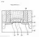
FIG. 2 is a cross-sectional view showing a structure of a dual interlayer dielectric layer of a semiconductor device according to a preferred embodiment consistent with the present invention.
Referring to FIG. 2, an isolation layer 21 such as STI (shallow trench isolation) is formed on a silicon substrate 20, thereby defining an active region. A gate oxide layer 22 and a gate 23 are formed on silicon substrate 20, and a sidewall spacer 24 is formed on the both sidewalls of gate 23. A source/drain region 25 is formed in the active region of silicon substrate 20, and a silicide (not shown) is formed on source/drain region 25 and gate 23, respectively.
Etch stop layer 26 is formed in such a manner as to cover the entire structure, and interlayer dielectric layers 27a and 27b of a dual layer structure are sequentially stacked on etch stop layer 26. A contact hole is formed by selectively etching interlayer dielectric layers 27a and 27b, and a contact is formed by depositing a conductive material (e.g., tungsten) into the contact hole.
In such a structure, etch stop layer 26 is made of silicon nitride in the same manner as the conventional invention. Further, interlayer dielectric layers 27a and 27b may include ozone Tetraethoxysilane (hereinafter, referred to as O3-TEOS layer) and plasma-enhanced Tetraethoxysilane (hereinafter, refers to as PE-TEOS layer), respectively.
O3-TEOS layer 27a directly abuts against etch stop 26 and has an excellent gap fill capacity and functions to relieve compressive stress.
Interlayer dielectric layers 27a and 27b according to a preferred embodiment consistent with the invention may be formed by a method and which will be described below.
O3-TEOS layer 27a is deposited on a structure including etch stop layer 26 deposited therein. The deposition condition of the O3-TEOS layer is as follows:
TEOS: 1000 mgm±10%; O3: 4500 sccm±10%; N2: 4000 sccm; He: 2000 sccm; temperature: 480° C.; and pressure: 500 Torr.
O3-TEOS layer (27a) is then flattened using a chemical mechanical polishing (CMP) process, and then PE-TEOS layer 27b is deposited on O3-TEOS layer 27a. The deposition condition of PE-TEOS layer 27b is as follows:
TEOS: 950±100 mgm; O2: 840±50 sccm; He: 560±50 sccm; temperature: 400° C.; pressure: 5 Torr; HF electric power: 550±25 W; and LF electric power: 125±10 W.
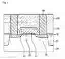
The dual interlayer dielectric layer consistent with the present invention may have another structure. FIG. 3 is a cross-sectional view showing a structure of a dual interlayer dielectric layer of a semiconductor device according to another preferred embodiment consistent with the present invention.
Referring to FIG. 3, the other components except for the interlayer dielectric layer are identical to that of the preferred embodiment as described above. Accordingly, the description of the same reference numerals will be omitted since they are used to denote identical elements having the same functions throughout the drawings. Interlayer dielectric layers 37a and 37b of a dual layer structure, which are sequentially formed on etch stop layer 26, include a PE-TEOS layer 37a and a HDP-CVD layer 37b, respectively.
When PE-TEOS layer 37a is shallowly deposited on etch stop layer 26 before depositing HDP-CVD layer 37b, PE-TEOS layer 37a can prevent a delamination phenomenon generated between etch stop layer 26 and HDP-CVD layer 37b while acting as an adhesion layer.
Interlayer dielectric layers 37a and 37b according to a preferred embodiment consistent with the invention may be formed by a method and which will be described below.
PE-TEOS layer 37a is deposited on a structure including etch stop layer 26. A deposition condition of the PE-TEOS layer is identical to that of PE-TEOS layer (27b) according to a preferred embodiment consistent with the invention as described above. However, only the time of the deposition is adjusted in order to obtain thin deposition thickness.
HDP-CVD layer 37b is deposited on deposited PE-TEOS layer 37a. The deposition condition of HDP-CVD layer 37b is as follows:
Ar: 110 sccm±10% (side), 16 sccm±10% (top); O2: 100˜140 sccm (side), 15˜20 sccm (top); SiH4: 45˜65 sccm (side), 8˜11 sccm (top); Pressure: throttle valve is fully opened; RF electrical power: 1300 W±10% (top), 3100 W±10% (side), 2400˜3100 W (bias).
As described above, according to a structure of a dual interlayer dielectric layer and a method for forming the same consistent with the present invention, the O3-TEOS layer having an excellent gap fill capacity and adapted for relieving compressive stress is formed on the etch stop layer, so that an interlayer delamination phenomenon can be prevented from being generated between the etch stop layer and the interlayer dielectric layer, and the contact material may be prevented from penetrating in the following contact material deposition process.
Further, according to a structure of a dual interlayer dielectric layer and a method for forming the same consistent with the present invention, the thin PE-TEOS layer functioning as an adhesion layer is formed on the etch stop layer, so that an adhering force between the etch stop layer and the interlayer dielectric layer can be improved, thereby preventing the interlayer delamination phenomenon generated between the etch stop layer and the interlayer dielectric layer.
It will be apparent to those skilled in the art that various changes and modifications may be made without departing from the spirit and scope consistent with the invention and the following claims.
Claims
What is claimed is:1. A method for forming a dual interlayer dielectric layer of a semiconductor device comprising:
forming an etch stop layer on a substrate, the substrate having a source/drain region and a gate formed thereon;
depositing a first interlayer dielectric layer including O3-TEOS on the etch stop layer;
planarizing the first interlayer dielectric layer;
depositing a second interlayer dielectric layer including PE-TEOS on the first interlayer dielectric layer; and
forming a contact by selectively etching the first interlayer dielectric layer and the second interlayer dielectric layer and depositing a conductive material thereon.
2. The method according to claim 1, wherein the etch stop layer includes silicon nitride.
3. The method according to claim 1, wherein depositing the first interlayer dielectric layer comprises performing a deposition process under conditions including: TEOS: 1000 mgm±10%; O3: 4500 sccm±10%; N2: 4000 sccm; He: 2000 sccm; temperature: 480° C.; and pressure: 500 Torr.
4. The method according to claim 1, wherein depositing the second interlayer dielectric layer comprises performing a deposition process under conditions including: TEOS: 950±100 mgm; O2: 840±50 sccm; He: 560±50 sccm; temperature: 400° C.; pressure: 5 Torr; HF electric power: 550±25 W; and LF electric power: 125±10 W.
5. A method for forming a dual interlayer dielectric layer of a semiconductor device, the method comprising:
forming an etch stop layer on a substrate, the substrate having a source/drain region and a gate formed therein;
depositing a first interlayer dielectric layer formed of PE-TEOS on the etch stop layer;
depositing a second interlayer dielectric layer formed of HDP-CVD on the first interlayer dielectric layer; and
forming a contact by selectively etching the first interlayer dielectric layer and the second interlayer dielectric layer and depositing a conductive material thereon.
6. The method according to claim 5, wherein the etch stop layer includes silicon nitride.
7. The method according to claim 5, wherein depositing the first interlayer dielectric layer comprises performing a deposition process under conditions including: TEOS: 950±100 mgm; O2: 840±50 sccm; He: 560±50 sccm; temperature: 400° C.; pressure: 5 Torr; HF electric power: 550±25 W; and LF electric power: 125±10 W.
8. The method according to claim 5, wherein depositing the second interlayer dielectric layer comprises performing a deposition process under condition including: Ar: 110 sccm±10% (side), 16 sccm±10% (top); O2: 100˜140 sccm (side), 15˜20 sccm (top); SiH4: 45˜65 sccm (side), 8-11 sccm (top); pressure: throttle valve is fully opened; RF electric power: 1300 W±10% (top), 3100 W±10% (side), 2400˜3100 W (bias).
Images & Drawings included:
Sources:
- United States Patent and Trademark Office - verify current appl. status at the USPTO↗
Recent applications in this class:
- » 20250266294 2025-08-21
METHODS FOR DEPOSITING SILICON OXIDE - » 20250259888 2025-08-14
METHODS FOR DEPOSITING GAP FILLING FLUIDS AND RELATED SYSTEMS AND DEVICES - » 20250233017 2025-07-17
GAP-FILLING METHOD FOR A SEMICONDUCTOR DEVICE AND METHOD OF MANUFACTURING A SEMICONDUCTOR DEVICE USING THE SAME - » 20250201628 2025-06-19
METHODS FOR DEPOSITING GAP FILLING FLUIDS AND RELATED SYSTEMS AND DEVICES - » 20250038048 2025-01-30
SUBSTRATE PROCESSING METHOD - » 20240395610 2024-11-28
STRUCTURES FOR REDUCING GAP FILL DEFECTS IN A VERTICALLY STACKED SEMICONDUCTOR DEVICE AND METHODS FOR FORMING THE SAME - » 20240379420 2024-11-14
METHOD OF DIELECTRIC MATERIAL FILL AND TREATMENT - » 20240379419 2024-11-14
SEMICONDUCTOR STRUCTURE HAVING SEAM SEALED - » 20240371690 2024-11-07
SEMICONDUCTOR DEVICE STRUCTURE AND METHODS OF FORMING THE SAME - » 20240312836 2024-09-19
INTEGRATED CIRCUIT PACKAGES AND METHODS OF FORMING THE SAME
Recent applications for this Assignee:
- » 20100314675 2010-12-16
Power semiconductor device and method for manufacturing the same - » 20100133421 2010-06-03
Complementary metal oxide silicon image sensor and method of fabricating the same - » 20100029051 2010-02-04
Semiconductor device and fabricating method thereof - » 20100019353 2010-01-28
Semiconductor device and method for manufacturing the same - » 20090317953 2009-12-24
Memory device and method for manufacturing the same - » 20090317952 2009-12-24
Memory device and method for manufacturing the same - » 20090317949 2009-12-24
ESD protecting circuit and manufacturing method thereof - » 20090302361 2009-12-10
Complementary metal oxide semiconductor (CMOS) image sensor - » 20090278205 2009-11-12
High voltage BICMOS device and method for manufacturing the same - » 20090273032 2009-11-05
LDMOS device and method for manufacturing the same