Doubled-sided pluggable backplane
US20070178718A1
2007-08-02
10/554,545
2004-01-05
✅ Patent granted
US 7,433,195 B2
2008-10-07
WO; PCT/CN2004/000016; 20040105
WO; WO2004/097990; 20041111
Michael C. Zarroli
2024-01-05
Abstract:
The invention discloses a double-sided pluggable backplane, having one side on which one or more than one front backplane connector is disposed according to width of plot positions and the other side on which one or more than one rear backplane connector is disposed according to width of plot positions, the front backplane connector and the adjacent rear backplane connector being located at the same horizontal level on the double-sided pluggable backplane and staggered right-and-left in turn, meanwhile the front backplane connector and the rear backplane connector having uniform specifications and the same contact pin definitions. The double-sided pluggable backplane according to the present invention can realize interchangeability of front boards and rear boards and have no special requirements for design and manufacture of printed circuit boards and machining of the backplane, which decreases cost of production and difficulty on processing. At the same time, interchangeability of front boards and rear boards reduces design cost of boards.
Inventors:
- Zhenya Li 3 🇨🇳 Guangdong, China
- Konggang Wei 1 🇨🇳 Guangdong, China
- Wenjian Li 1 🇨🇳 Guangdong, China
- Chenglong Wang 2 🇨🇳 Guangdong, China
- Guzheng Wu 1 🇨🇳 Guangdong, China
- Zhiguo Yang 1 🇨🇳 Guangdong, China
- Junwen Jin 1 🇨🇳 Guangdong, China
Assignee:
- HUAWEI TECHNOLOGIES CO., LTD. 612 🇨🇳 Shenzhen Guangdong, China
Interested in similar patents?
Get notified when new applications in this technology area are published.
Classification:
H01R12/52 » CPC main
Structural associations of a plurality of mutually-insulated electrical connecting elements, specially adapted for printed circuits, e.g. printed circuit boards [PCBs], flat or ribbon cables, or like generally planar structures, e.g. terminal strips, terminal blocks; Coupling devices specially adapted for printed circuits, flat or ribbon cables, or like generally planar structures; Terminals specially adapted for contact with, or insertion into, printed circuits, flat or ribbon cables, or like generally planar structures; Fixed connections for rigid printed circuits or like structures connecting to other rigid printed circuits or like structures
H05K1/18 » CPC further
Printed circuits Printed circuits structurally associated with non-printed electric components
H05K1/18 » CPC further
Printed circuits Printed circuits structurally associated with non-printed electric components
H01R31/06 » CPC further
Coupling parts supported only by co-operation with counterpart Intermediate parts for linking two coupling parts, e.g. adapter
H05K2201/044 » CPC further
Indexing scheme relating to printed circuits covered by; Assemblies of printed circuits Details of backplane or midplane for mounting orthogonal PCBs
H05K2201/044 » CPC further
Indexing scheme relating to printed circuits covered by; Assemblies of printed circuits Details of backplane or midplane for mounting orthogonal PCBs
H05K2201/097 » CPC further
Indexing scheme relating to printed circuits covered by; Shape and layout; Shape and layout details of conductors covering at least two types of conductors provided for in - Alternating conductors, e.g. alternating different shaped pads, twisted pairs; Alternating components
H05K2201/10189 » CPC further
Indexing scheme relating to printed circuits covered by; Details of components or other objects attached to or integrated in a printed circuit board; Types of components Non-printed connector
H05K2201/10189 » CPC further
Indexing scheme relating to printed circuits covered by; Details of components or other objects attached to or integrated in a printed circuit board; Types of components Non-printed connector
H05K2203/1572 » CPC further
Indexing scheme relating to apparatus or processes for manufacturing printed circuits covered by; Position of the PCB during processing Processing both sides of a PCB by the same process; Providing a similar arrangement of components on both sides; Making interlayer connections from two sides
H05K1/00 IPC
Printed circuits
H05K1/00 IPC
Printed circuits
H05K1/14 IPC
Printed circuits; Details Structural association of two or more printed circuits
H05K1/14 IPC
Printed circuits; Details Structural association of two or more printed circuits
Description
FIELD OF THE TECHNOLOGYThe invention relates to a backplane used in a communication device, in particular to a double-sided pluggable backplane.
BACKGROUND OF THE INVENTIONAt present, with high requirements for integration of a communication system, it has become a developing trend to directly multiply the number of slots with a double-sided pluggable backplane in backplane technology. Multiplication of the number of slots improves balancing of configuration granularity of system services on a board, directly leading to flexibility and reliability of design as well as feasibility for multi-production integration.
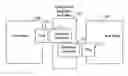
FIG. 1 schematically illustrates connection of a double-sided pluggable backplane and boards according to the prior art. As shown in FIG. 1, a front board 100 is plugged into a front backplane connector 111 of a double-sided pluggable backplane 110 by means of a plug 101, and a rear board 120 is plugged into a rear backplane connector 112 of the double-sided pluggable backplane 110 by means of a plug 121. Front board 100 is in alignment with the corresponding rear board 120. However, front backplane connector 111 and rear backplane connector 112 are located at different horizontal levels, meanwhile plug 101 of front board 100 and plug 121 of rear board 120 are located at different horizontal levels too, i.e. they are staggered up-and-down. Although front backplane connector 111 and rear backplane connector 112 can have uniform definitions for interface contact pins, yet they have different horizontal locations, thus front board 100 and rear board 120 can not be interchangeable on a double-sided pluggable backplane.
It could be seen this kind of double-sided pluggable backplane has an insurmountable disadvantage. More specifically, a board in a front slot cannot be interchanged with that in a rear slot, which is similar to back-to-back integration of two frames in essence.
Aiming at the above disadvantage, a design idea has been proposed that adopts special backplane connectors to make boards interchangeable at fore-and-aft slot positions.
FIG. 2 is a schematic diagram illustrating an interchangeable double-sided pluggable backplane and boards according to the prior art. As shown, a front board 200 is plugged into a front backplane connector 211 of a double-sided pluggable backplane 210 by means of a plug 201, and a back board 220 is plugged into a rear backplane connector 212 of double-sided pluggable backplane 210 by means of a plug 221. Both of front backplane connector 211 and rear backplane connector 212 comprise a power supply interface and a signal interface, and they are located at the same horizontal level. Meanwhile, front backplane connector 211 and rear backplane connector 212 have uniform definitions for interface contact pins, so front board 200 and rear board 220 are interchangeable on the backplane.
Here, front backplane connector 211 and rear backplane connector 212 on double-sided pluggable backplane are the same special backplane connectors, and they are aligned in the up-and-down position and fore-and-aft position absolutely. The depth of the contact pins of front backplane connector 211 and rear backplane connector 212 must be less than or approximately equal to half of the thickness of the backplane, and the contact pins must be insulated from each other.
The above-mentioned double-sided pluggable backplane has rather high requirements for its circuit board. The thickness error of the circuit board must be exceedingly tiny, otherwise it cannot be guaranteed that the depth of the contact pins of the special backplane connectors is less than or approximately equal to half of the thickness of the backplane and that the contact pins are insulated from each other. The speciality of the backplane connector, along with the special requirements for designing, manufacturing of the printed circuit board in the backplane and machining of the backplane directly bring about some insurmountable difficulties, such as costliness, difficulty in processing and so on. Therefore this kind of double-sided pluggable backplane is still in the stage of designing rather than being applied in practical manufacturing.
SUMMARY OF THE INVENTIONIn view of this, an object of the invention is to provide a double-sided pluggable backplane which can realize interchangeability of front boards and rear boards, reduce design and manufacture difficulty of the double-sided pluggable backplane and lowers design cost of the board.
To achieve the above object, the technical scheme of the present invention is implemented as follows.
A double-sided pluggable backplane has one side on which one or more than one front backplane connector is disposed according to width of plot positions and the other side on which one or more than one rear backplane connector is disposed according to width of plot positions. The front backplane connector and the adjacent rear backplane connector are located at the same horizontal level on the double-sided pluggable backplane and staggered right-and-left in turn. Meanwhile the front backplane connector and the rear backplane connector have uniform specifications and the same contact pin definitions.
The front backplane connector and the adjacent rear backplane connector may share width of one slot position.
Each of the front and rear backplane connectors may comprise a power supply interface connector and a signal interface connector.
Both the power supply interface connector and the signal interface connector may be common backplane connectors.
Each of the front and rear backplane connectors may comprise guiding/error-preventing pins on upper end and lower end.
From the above technical scheme of this invention, it can be seen that the double-sided pluggable backplane according to the present invention can realize interchangeability of front boards and rear boards easily with common backplane connectors by staggering the front and rear backplane connectors left-and-right. The double-sided pluggable backplane according to the invention has no special requirements for design and manufacture of printed circuit boards and machining of the backplane, which decreases cost of production and difficulty on processing. At the same time, interchangeability of front boards and rear boards reduces design cost of boards.
BRIEF DESCRIPTION OF THE DRAWINGSFIG. 1 is a schematic diagram illustrating connection between a double-sided pluggable backplane and boards according to the prior art.
FIG. 2 is a schematic diagram illustrating an interchangeable double-sided pluggable backplane and boards according to the prior art.
FIG. 3 is a schematic top view illustrating a double-sided pluggable backplane according to a preferred embodiment of the present invention.
FIG. 4 is a schematic front view illustrating the double-sided pluggable backplane shown in FIG. 3.
DETAILED DESCRIPTION OF THE INVENTIONNow, the present invention will be described in detail hereinafter with reference to an embodiment and accompanying drawings.
It is not necessary to adopt special connectors for double-sided pluggable backplane on the double-sided pluggable backplane according to the invention. Instead, narrow backplane connectors may be adopted. In an embodiment, common ZD connectors may be employed. The width sum of two connectors may approximately equal to the width of one slot position. In this invention, it is not required that the width sum of the two connectors accurately equals to the width of one slot position, and thus this invention can be realized with various kinds of common connectors, leading to easiness and flexibility in implementations.
FIG. 3 is a schematic top view illustrating a double-sided pluggable backplane according to a preferred embodiment of the present invention. As shown in FIG. 3, in an interval of an approximate one slot position on a double-sided pluggable backplane 300, the left half of the interval is occupied by a front backplane connector 301, and the right half of it is occupied by a rear backplane connector 311. Obviously, the right half of the interval may be occupied by front backplane connector 301, and the left half of it may be occupied by rear backplane connector 311.
If the interval of one slot position is not enough for the width sum of two backplane connectors, the front and the back slot positions may be staggered left-and-right in order to ensure the double-sided connector being installed horizontally. Generally, male connectors are adopted on the front and rear backplane connectors of the double-sided pluggable backplane, and female connectors are adopted on boards.
FIG. 4 is a schematic front view illustrating the double-sided pluggable backplane shown in FIG. 3. As shown in FIG. 4, the front backplane connector and the rear backplane connector on the double-sided pluggable backplane in this embodiment respectively comprise a power supply interface connector and a signal interface connector which is a common ZD connector. The front backplane connector of double-sided pluggable backplane 400 according to the present embodiment comprises a power supply interface connector 401 and a signal interface connector 402. Power supply interface connector 401 can be located either above signal interface connector 402 or below it, providing the interface contact pin definitions of the backplane connector are the same as those of the board. In FIG. 4, reference sign 403 denotes a power supply interface connector of a rear backplane connector, while reference sign 404 denotes a signal interface connector of the rear backplane connector. Power supply interface connector 403 is identical and disposed at the same horizontal level with power supply interface connector 401 while signal interface connector 404 is identical and disposed at the same horizontal level with signal interface connector 402, and identical interface connectors have absolutely uniform contact pin definitions.
To exactly plug the boards into the front/rear backplane connectors of the double-sided pluggable backplane, guiding/error-preventing pins are set on both the upper end and lower end of each front/rear backplane connector in this embodiment. The guiding/error-preventing pins may be set at other positions of the front/back backplane connector according to practical conditions.
It can be seen the front and rear backplane connectors of the both-sided pluggable backplane according to this embodiment are disposed at the same horizontal level and have uniform contact pin definitions, which makes it not necessary to design front boards and rear boards respectively. Since the front and rear backplane connectors usually employ male connectors, the only requirement for connectors on boards is that they employ female connectors corresponding to the male connectors of the front and rear backplane connectors, thus interchangeability of the front board and the rear board is achieved and design cost for boards is lowered.
In addition, in this embodiment, the number of front backplane connectors on the both-sided pluggable backplane can be either the same as or different from the number of rear backplane connectors according to the actual requirements of communication services.
It can be seen from the above embodiment that the double-sided pluggable backplane according to the present invention can realize interchangeability between front boards and rear boards easily with common backplane connectors. The double-sided pluggable backplane according to the invention has no special requirements for design and manufacture of printed circuit boards and machining of the backplane, which decreases cost of production and difficulty on processing. At the same time, interchangeability of front boards and rear boards reduces design cost of boards.
Claims
1. A double-sided pluggable backplane, having one side on which one or more than one front backplane connector is disposed according to width of plot positions and the other side on which one or more than one rear backplane connector is disposed according to width of plot positions, wherein said front backplane connector and the adjacent rear backplane connector are located at the same horizontal level on the double-sided pluggable backplane and are staggered right-and-left in turn; said front backplane connector and said rear backplane connector have uniform specifications and the same contact pin definitions.
2. The double-sided pluggable backplane of claim 1, wherein said front backplane connector and the adjacent rear backplane connector share width of one slot position.
3. The double-sided pluggable backplane of claim 1, wherein each of said front and rear backplane connectors comprises a power supply interface connector and a signal interface connector.
4. The double-sided pluggable backplane of claim 3, wherein both said power supply interface connector and said signal interface connector are common backplane connectors.
5. The double-sided pluggable backplane of claim 1, wherein each of said front and rear backplane connectors comprises guiding/error-preventing pins on an upper end and a lower end.
Images & Drawings included:


Sources:
- United States Patent and Trademark Office - verify current appl. status at the USPTO↗
Recent applications in this class:
- » 20250273884 2025-08-28
Interconnection System with Electromagnetic Absorber with Improved Performance - » 20250125546 2025-04-17
CONNECTOR INCLUDING SIGNAL PINS SHIELDED BY BURIED GROUND VIAS - » 20240405459 2024-12-05
Modular Printed Circuit Boards with Connectors - » 20240388018 2024-11-21
LIQUID METAL PATCH INTERCONNECT FOR LARGE WARPAGE COMPONENTS - » 20240291181 2024-08-29
BOARD-TO-BOARD CONNECTION STRUCTURE FOR PCB - » 20240291180 2024-08-29
Bus Bar Subassembly and Electrical Assembly - » 20240235071 2024-07-11
CIRCUIT MODULE - » 20240170867 2024-05-23
Connector including signal pins shielded by buried ground vias - » 20240136739 2024-04-25
CIRCUIT MODULE - » 20230420874 2023-12-28
ELECTRICAL CONNECTOR WITH HIGH SPEED MOUNTING INTERFACE
Recent applications for this Assignee:
- » 20250096876 2025-03-20
METHODS AND SYSTEMS FOR RECEIVE AND TRANSMIT BEAM PAIRING IN FULL DUPLEX SYSTEMS - » 20250014844 2025-01-09
OPEN BUTTON AND ELECTRONIC DEVICE - » 20240377521 2024-11-14
SENSING-ASSISTED POSITIONING OF MOBILE DEVICES - » 20240372635 2024-11-07
SYSTEMS AND METHODS FOR WIRELESS SIGNAL CONFIGURATION BY A NEURAL NETWORK - » 20240296144 2024-09-05
File storage location determining method and apparatus, and terminal - » 20240295945 2024-09-05
METHOD, ELECTRONIC DEVICE, AND SYSTEM FOR CREATING APPLICATION SHORTCUT - » 20240187486 2024-06-06
EXTENDED REALITY DATA TRANSMISSION METHOD AND APPARATUS - » 20240152310 2024-05-09
MULTI-DEVICE-BASED ONLINE INTERACTION METHOD, CHIP, ELECTRONIC DEVICE, AND STORAGE MEDIUM - » 20240111403 2024-04-04
PAGE SLIDING PROCESSING METHOD AND RELATED APPARATUS - » 20240089044 2024-03-14
FLEXIBLE FRAME STRUCTURE FOR WIRELESS COMMUNICATION