Force sensor
US20070186665A1
2007-08-16
10/591,879
2004-12-22
✅ Patent granted
US 7,404,338 B2
2008-07-29
WO; PCT/EP2004/014570; 20041222
WO; WO2005/095997; 20051013
Edward Lefkowitz | Punam Patel
2024-12-22
Abstract:
The resolution and the signal-to-noise ration of known force sensors as e.g. capacitive force sensors decrease when scaling them down. To solve this problem there is a solution presented by the usage of a nanostructure as e.g. a carbon nanotube, which is mechanically deformed by a force to be measured. The proposed force sensors comprises a support with two arms carrying the carbon nanotube. The main advantage of this nanoscale force sensor is a very high sensitivity as the conductance of carbon nanotubes changes several orders of magnitude when a mechanical deformation arises.
Inventors:
- Christoph Stampfer 2 🇮🇹 Vols am Schlern, Italy
- Christofer Hierold 2 🇨🇭 Hombrechtikon, Switzerland
- Alain Jungen 1 🇨🇭 Zurich, Switzerland
Assignee:
- ETH ZURICH 367 🇨🇭 Zurich, Switzerland
Interested in similar patents?
Get notified when new applications in this technology area are published.
Classification:
G01L1/04 IPC
Measuring force or stress, in general by measuring elastic deformation of gauges, e.g. of springs
B81B3/0021 » CPC main
Devices comprising flexible or deformable elements, e.g. comprising elastic tongues or membranes; Structures acting upon the moving or flexible element for transforming energy into mechanical movement or , i.e. actuators, sensors, generators Transducers for transforming electrical into mechanical energy or
B82Y15/00 » CPC further
Nanotechnology for interacting, sensing or actuating, e.g. quantum dots as markers in protein assays or molecular motors
G01L1/005 » CPC further
Measuring force or stress, in general by electrical means and not provided for in -
G01P15/123 » CPC further
Measuring acceleration; Measuring deceleration; Measuring shock, i.e. sudden change of acceleration by making use of inertia forces using solid seismic masses with conversion into electric or magnetic values by alteration of electrical resistance by piezo-resistive elements, e.g. semiconductor strain gauges
B81B2201/025 » CPC further
Specific applications of microelectromechanical systems; Sensors; Inertial sensors Inertial sensors not provided for in -
B82Y30/00 » CPC further
Nanotechnology for materials or surface science, e.g. nanocomposites
Y10S977/724 » CPC further
Nanotechnology; Nanostructure Devices having flexible or movable element
Y10S977/953 » CPC further
Nanotechnology; Specified use of nanostructure for electronic or optoelectronic application Detector using nanostructure
Y10S977/956 » CPC further
Nanotechnology; Specified use of nanostructure for electronic or optoelectronic application; Detector using nanostructure Of mechanical property
G01B7/16 IPC
Measuring arrangements characterised by the use of electric or magnetic means for measuring the deformation in a solid, e.g. by resistance strain gauge
G01P15/08 IPC
Measuring acceleration; Measuring deceleration; Measuring shock, i.e. sudden change of acceleration by making use of inertia forces using solid seismic masses with conversion into electric or magnetic values
Description
This invention relates to a force sensor according to the preamble of claim 1.
The present invention covers the field of measuring a force with a system in the micro- or nano-regime. Micro electro-mechanical force sensors are available in a plurality of principles. They differ by the detection mechanisms. Known sensors are based on piezoresistive, capacitive, tunnel current or thermal principles. These know force sensors are relatively large, that is they have large dimensions as some multiples of 100 μm. Force sensors according to the state-of-the-art are disclosed in the documents [5] and [6], in which limits to its size that is limits to a further miniaturization can be derived. In the context of the present invention force sensors are also denoted by <<inertial sensors>>.
In paper [1] furthermore all the problems which arise due to the increasing miniaturization of force sensors are discussed. The principle of a capacitive force sensor is depicted in FIG. 4(a): Due to the influence of a force
F=m·a,
where m denotes the mass and a the effecting acceleration, a change Δx of the distance x0 of two electrodes or plates A will occur. The capacity C is also determined by the dielectric constant ∈0 as well as by number ∈r, which is determined by the dielectric material between the plates A. These capacitive sensors show in general a degradation of the resolution by miniaturization. This effect results one the one hand from a not very suitable signal to noise ratio (SNR). On the other hand the actual cause is an over proportional scaling down of the forces as well as restrictions due to process limitations and design rules. They are also called miniaturization barriers. The limitations prevent that the scaling down of forces can be compensated by a corresponding miniaturization of the distance x0 of the electrodes.
A numeric example explains the draw back of the state-of-the-art sensor according to FIG. 4(a):
-
- x0=1 μm;
- Δx=0.05 μm;
- C0=0.53 pF;
- A=6·104 μm2.
The displacement of the plates by Δx=0.05 μm results in a relative change of capacitance ΔCrel≈5%.
Furthermore the increasing miniaturization of force sensors leads to the problem of a reduction of the gauge factor for measuring a force. For a capacitive force sensor a limit arises also in reduction of its seismic mass due to design rules.
The present invention therefore addresses the problem due to the miniaturization of force sensors.
The object of the present invention is to overcome the problems presented by the prior force sensors, especially to the degradation of the resolution.
These problems resulting from a further miniaturization are solved by a force sensor specified in claim 1.
By the proposed use of a nanostructure as e.g. a carbon nanotube a force sensor is provided, which increases significantly the sensitivity as well as the resolution. This improvements result from on the sensing principle based on quantum-mechanical effects. By a deformation of a nanostructure its electrical conductance is affected up to two orders of magnitude. This outstanding sensitivity of a nanostructure as e.g. a carbon nanotube is disclosed in [2].
Further advantageous embodiments are given in dependant claims.
The invention will be now described in preferred embodiments with reference to the accompanying drawings wherein:
FIG. 1 is a view of a first embodiment;
FIG. 2 is a view of a first embodiment, which allows a compensation of environmental effects;
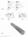
FIG. 3(a), FIG. 3(b) show the principle of the deformation of a carbon nanotube;
FIG. 4(a) shows the principle of a known capacitive force sensor;
FIG. 4(b) discloses the principle of a force sensor according to the present invention;
FIG. 5 shows a carbon nanotube.
FIG. 5 illustrates the topological structure of a carbon nanotube. The aspect ratio of common carbon nanotubes is in the range 50 . . . 5000. An example of the length is given below. Before explaining embodiments the properties of carbon nanotubes are first briefly discussed and references to its properties and production are given.
The invention becomes apparent by considering the sensitivity of a carbon nanotube when being object of a deformation caused by a force F. Sensitivity is in this context the ratio
ΔG/ΔF
where
-
- ΔG: change of conductance.
- ΔF: change of force.
For a carbon nanotube 3 the conductance G instead of the capacitance C is the electrical property, which is affected by the resulting deformation caused by a force. The sensitivity of a carbon nanotube 3 is up to two orders of magnitude compared to the sensitivity of a capacitive force sensor. This outstanding sensitivity and its possible causes are discussed and disclosed in the document [2].
Corresponding to the values given in the introduction of this document the sensitivity of a force sensor 1 with a carbon nanotube of height h is approximately as follows:
-
- h=0.600 μm;
- Δx=0.050 μm;
- F=8 nN;
- ΔGrel=99%.
In the publication [3] in an extensive manner the synthesis, properties and possible applications of carbon nanotubes 3 are disclosed. The teachings of this document [3] are therefore here incorporated by reference to it.
The principle of a force sensor 1 according the present invention is depicted in FIG. 3(a), 3(b) and 4(b). According to the representation in FIG. 3(a) and 3(b) a force F acts on carbon nanotube 5. A carbon nanotube 5 is carried or fixed between two arms 4. The carbon nanotube 5 itself is part of a electric circuit with a current I. A deformation Δx caused by a force F perpendicular to the carbon nanotube 3 decreases its conductance G. This results by a voltage driven measurement in a lowering of current I. The amount of the current I gives an indirect measure of the acting force F. By an external circuitry and an appropriate calibration the size of the force F can be displayed. The force F is either from an external source or caused by an movable element, which is a part of the force sensor 1. The latter principle is depicted in FIG. 4(b), where the movement of the element 7 is caused by an acceleration.
In table 1 shows an example of the dimensions and its parameters of a carbon nanotube, which is the basic element of the present invention. The cited values correspond to those disclosed in [2], the symbol S denotes the unit Siemens, the unit for conductance G:
| TABLE 1 |
| typical parameters of a carbon nanotube. |
| Dimension, parameter | Value | |
| Length of a carbon nanotube | 500 | nm | |
| force acting perpendicular to the axis | 8 | nN | |
| of a carbon nanotube | |||
| displacement, deformation Δx | 50 | nm |
| conductance change ΔG | 9 · 10−6 S to 9 · 10−8 S | |
For a force sensor 1 according to the present invention the carbon nanotube 3 may built on the basis of a chemical vapour deposition process CVD as controlled growth on prepatterned nanostructures. Details to this processes can be derived from document [4].
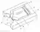
FIG. 1 shows a g-sensor 1—acceleration sensor—as a first embodiment of the present invention. The sensor 1 includes a U-shaped support 2 of two arms 4 carrying carbon nanotube 3. The two arms 4 are electrically insulated at the position 6, partly shown in FIG. 1. A moveable element 7 of mass m is located between the arms 4. The moveable element 7 is provided with a cusp tip 11. A movement of the element 7 towards the carbon nanotube 3 is caused by a force F determined by
F=m·a,
where:
- m mass of element 7;
- a acceleration acting via sensor 1 on element 7.
Tip 11 transfers the force F on to the carbon nanotube 3, by which force the carbon nanotube is mechanically stressed, that is deformed by a value Δx.
Optionally (not shown in FIG. 1) the sensor 1 is provided with at least one stop element in order to limit the movement of element 7. These stop elements enable a improved shock resistance of the sensor 1. Each arm 4 is provided with a cusp 5, on which the carbon nanotube 3 is mounted.
The stability of the moveable element 7 may be increased by at least one spring 8. The spring 8 serves also for the guidance of the moveable element 7
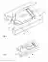
A further embodiment of the present invention is depicted in FIG. 2 with a second nanotube 10. The second carbon nanotube 10 may not be deformed by a force F. The arrangement with a second nanotube 10 allows the compensation of environmental effects as e.g. temperature. The second carbon nanotube is in mounted to the arms 4 in the same manner as described above. However the second carbon nanotube 10 is electrically insulated from the first one. The second carbon nanotube 10 is also part of an electric circuit with a current I. By an external circuitry this arrangement allows a common mode rejection, that is the above mentioned compensation of environmental effects. Also a possible deformation of the support 2 can be compensated by using a second carbon nanotube 10
Force sensors and g-sensors according to the present invention are especially suitable for Vehicle dynamic control systems, but this example of application is not limiting at all.
The outstanding sensitivity of a g-sensor 1 according to the present invention allows the detection of very small accelerations, which opens a broad field of applications.
The invention is not limited to the embodiment depicted above with a carbon nanotube. The invention can also be carried out with other elements which have similar properties as carbon nanotube. Another example is a bor-nitride nanotube. It shows a huge change in electrical and optical properties by mechanical deformation as it has been shown for carbon nanotubes
[1]. In a more general context nanotubes count to the material class of quasi one-dimensional (1D) nanostructures which are characterized by the confinement of electrons in two spatial directions. These strong effects even hold for a big class of nanostructures where local atomic bonds determine the electrical and optical properties.
Therefore in this paper the elements
-
- carbon nanotubes,
- nanotubes,
- quasi one-dimensional (1D) nanostructures are summarized by the general term <<nanostructure>>.
- 1 force sensor, inertial sensor
- 2 support
- 3 carbon nanotube, nanotube, bor-nitride nanotubes, quasi one-dimensional (1D) nanostructures; nanostructure
- 4 arm
- 5 cusp at the arm 4, mounting point of a carbon nanotube
- 6 insulation
- 7 moveable element, mass
- 8 spring
- 9 insulation between nanotube 3 and 10
- 10 second carbon nanotube, second nanotube, second bor-nitride nanotubes, second quasi one-dimensional (1D) nanostructures; second nanostructure
- 11 tip of the moveable element 7
List of Symbols - a acceleration [m/s2]
- ∈0 dielectric constant
- ∈r relative dielectric constant
- F force
- G conductance
- m mass [g]
- x0 distance, e.g. [μm or nm]
- Δx displacement, e.g. [μm or nm]
- ΔC change of capacity.
- ΔF change of force.
- ΔG change of conductance
List of Acronyms - CNT carbon nanotube
- CVD chemical vapour deposition
- MEMS Microelectromechanical systems
- SNR Signal to noise ratio
- VDC Vehicle dynamic control
- [1] C. Hierold,
- <<Micro- and Nanosystems: Review and Outlook>>, MME 2003, 14th Micromechanics Europe Workshop, Delft, 2003.
- [2] S T. W. Tombler et al.,
- <<Reversible electromechanical characteristics of carbon nanotubes under loca-probe manipulation>>
- Nature 405, 769 (2000)
- [3] S. B. Sinnott and R. Andrews,
- <<Carbon Nantubes: Synthesis, properties and applications>>
- Critical Reviews in Solid State and Material Science, 26 (3), 145 (2001)
- [4] N. R. Franklin and H. Dai,
- <<An enhanced CVD approach to extensive nanotube networks with directionality>>
- Advanced Materials, 12, 890, (2000)
- [5] C. Acar and A. M. Shkel,
- <<Experimental evaluation and comparative analysis of commercial variable-capacitance MEMS accelerometers>>Journal of Micromechanics and Microengineering 13 634 (2003)
- [6] N. Yazdi, F. Ayazi, K. Najafi,
- <<Micromachined Inertial Sensors>>
- Proceeding of the IEEE, Vol. 86, No. 8, August 1998
Claims
1-11. (canceled)
12. A force sensor device, comprising:
a support of two arms carrying a longitudinal electromechanical element in form of a nanostructure, said nanostructure having electric properties changeable in response to a mechanical deformation due to a force; and
an actuator disposed to transmit a force to said nanostructure.
13. The force sensor device according to claim 12, wherein said nanostructure is a structure selected from the group consisting of a nanotube, a carbon nanotube, a boron-nitride nanotube, and a quasi one-dimensional nanostructure.
14. The force sensor device according to claim 12, wherein the changeable electric property is a conductivity of said nanostructure.
15. The force sensor device according to claim 12, wherein said support is a U-shaped support.
16. The force sensor device according to claim 12, wherein each of said two arms is formed with a cusp and said nanostructure is mounted to said cusp.
17. The force sensor device according to claim 12, which further comprises a movable mass formed with a tip disposed between said two arms, and wherein said mass is disposed to be movable due to an acting acceleration and said tip is disposed to act on said nanostructure due to a resulting force.
18. The force sensor device according to claim 12, wherein said nanostructure is a first nanostructure and a second nanostructure is carried by said arms for compensating for environmental effects.
19. The force sensor device according to claim 18, wherein each of said two arms is formed with a cusp carrying said first nanostructure and with a cusp carrying said second nanostructure.
20. The force sensor device according to claim 18, which further comprises an insulation formed on at least one of said arms for electrically separating said nanostructures.
21. The force sensor device according to claim 18, wherein said second nanostructure is a nanotube, a carbon nanotube, or a quasi one-dimensional nanostructure.
Images & Drawings included:
Sources:
- United States Patent and Trademark Office - verify current appl. status at the USPTO↗
Similar patent applications:
- » 20240254352
FORCE SENSORS, FORCE SENSOR CONTROLLED ELECTRONICS, AND FORCE SENSOR CONTROLLED CONDUCTIVE HEATING ELEMENTS - » 20200173869
Force sensor, torque sensor, force-sense sensor, fingertip-force sensor, and method of manufacturing the same - » 20180372564
Multi-axial force sensor including piezoresistive groups, method of manufacturing the multi-axial force sensor, and method for operating the multi-axial force sensor - » 20210319198
Force sensor having force sensor electrodes, display device including the same, and method for driving the same - » 20080173106
Stress detection method for force sensor device with multiple axis sensor and force sensor device employing this method - » 20210285834
Force sensor and force sensor manufacturing method - » 20180141217
Force detection sensor, force sensor, torque sensor, and robot - » 20110259111
Temperature compensation method for force sensor and force sensor - » 20080066562
Chip for force sensor and force sensor - » 20240272024
FORCE SENSOR AND FORCE DETECTION SYSTEM PRESSING FORCE SENSOR
Recent applications in this class:
- » 20250282607 2025-09-11
INTEGRATED MEMS ELECTROSTATIC MICRO-SPEAKER DEVICE AND METHOD - » 20250250157 2025-08-07
MEMS TRANSDUCER - » 20250236507 2025-07-24
ALL-SILICON CARBIDE (SiC) ACCELERATION-PRESSURE INTEGRATED SENSOR CHIP AND PREPARATION METHOD THEREOF - » 20250236506 2025-07-24
MEMS DEVICE BUILT USING THE BEOL METAL LAYERS OF A SOLID STATE SEMICONDUCTOR PROCESS - » 20250223151 2025-07-10
SEMICONDUCTOR DEVICE AND AIRFLOW GENERATING PACKAGE - » 20250214829 2025-07-03
MICROELECTROMECHANICAL ACTUATOR ON INSULATING SUBSTRATE - » 20250197194 2025-06-19
THREE-DIMENSIONAL STRESS-SENSITIVE DEVICE - » 20250171294 2025-05-29
MEMS THIN MEMBRANE WITH STRESS STRUCTURE - » 20250136433 2025-05-01
MEMS DIE AND MEMS-BASED SENSOR - » 20250128934 2025-04-24
METHOD FOR SENSOR STATE DETECTION, ENVIRONMENTAL SENSOR SYSTEM AND MOBILE CONSUMER DEVICE
Recent applications for this Assignee:
- » 20250268954 2025-08-28
Treatment and/or Prevention of Digestive Disorder by a Bacterial Composition of Propionibacterium Freudenreichii and Bifidobacterium Longum - » 20250225676 2025-07-10
A METHOD FOR DETERMINING THE 6D POSE OF A CAMERA USED TO ACQUIRE AN IMAGE OF A SCENE USING A POINT CLOUD OF THE SCENE AND FEATURES - » 20250222166 2025-07-10
GRAFT SCAFFOLD FOR CARTILAGE REPAIR AND PROCESS FOR MAKING SAME - » 20250220781 2025-07-03
HEATING DEVICE FOR PREVENTING OR REMOVING A DEPOSITION - » 20250152713 2025-05-15
MULTICHAIN ANTIGEN-SPECIFIC RECEPTORS FOR CELL-BASED IMMUNOTHERAPY - » 20250093438 2025-03-20
MAGNETIC RESONANCE DEVICE COMPRISING A SAMPLE SPINNING APPARATUS - » 20250090583 2025-03-20
UNIVERSAL TCR VARIANTS FOR ALLOGENEIC IMMUNOTHERAPY - » 20250065307 2025-02-27
ADDITIVE MANUFACTURING OF STRUCTURES FOR USE IN A THERMOCHEMICAL FUEL PRODUCTION PROCESS - » 20250052761 2025-02-13
METHOD AND TOOLS FOR THE DETERMINATION OF CONFORMATIONS AND CONFORMATIONAL CHANGES OF PROTEINS AND OF DERIVATIVES THEREOF - » 20250025686 2025-01-23
DEVICE AND METHOD FOR ELECTRICALLY STIMULATING AT LEAST ONE NERVE