DIGITAL VIDEO BROADCASTING-HANDHELD RECEIVER AND RECEIVING METHOD
US20080101397A1
2008-05-01
11/554,810
2006-10-31
Abstract:
A digital video broadcasting-handheld (DVB-H) receiver and a receiving method therefore, in which DVB-H receiver includes a buffer unit, an error correction unit, an access unit, and a buffer arbitration unit. The buffer unit includes a plurality of memory regions and stores data in a first format of consecutively received burst data. The error correction unit performs error correction on the data in the first format. The access unit accesses the buffer unit to allow writing the data in the first format of the burst data. The buffer arbitration unit arbitrates access requests to the buffer unit. The access unit allows the data in the first format to be stored in the buffer unit through a dedicated access path. The DVB-H receiver can effectively process consecutively received elementary stream data using a multi protocol encapsulation buffer memory having a minimum capacity.
Interested in similar patents?
Get notified when new applications in this technology area are published.
Classification:
H04L12/56 IPC
Data switching networks; Store-and-forward switching systems Packet switching systems
Description
BACKGROUND OF THE INVENTION
1. Technical Field
The present disclosure relates to a digital video broadcasting-handheld (DVB-H) receiver, and more particularly, to a DVB-H receiver that can receive multiple services with the addition of only a minimum memory capacity, and a receiving method for the same.
2. Discussion of the Related Art
In DVB-T (Digital Video Broadcasting-Terrestrial), which is a European consortium standard for the broadcast transmission of digital terrestrial televisions broadcast data including video images and audio data is broadcast using orthogonal frequency division multiplexing (OFDM).
In addition, as portable devices, such as mobile phones, PDA, etc, are rapidly becoming popular, the desire to watch TV using a portable device is increasing. Since DVB-T was developed for a TV; receiving digital broadcasts, however, DVB-T is not suitable to be applied to portable devices. Thus, a new method suitable for watching TV broadcasts using a portable device is required.
DVB-H (Digital Video Broadcasting-Handheld), which was suggested in response to the above requirement, was developed based on the DVB-T standard. Accordingly, the DVB-T standard is aimed at multi-channel or high-definition (HD) services, while the DVB-H standard is aimed at providing standard definition (SD) moving images of 2 Mbps or less to allow a user moving at high speeds to view clear moving images.
The DVB-H standard uses a time-division method and an internet protocol (IP) datagram transmission method in which information is transmitted as packets according to the Internet Protocol (IP). A protocol architecture in the DVB-H standard includes a physical layer, a data link layer, and a network layer. The data link layer includes a multi protocol encapsulation (MPE) portion including an IP datagram or a multi protocol encapsulation-forward error correction (MPE-FEC) portion that performs error-correction coding.
According to the DVB-H standard, the MPE portion is batch transmitted as a frame using a time-slice method and a delta-T method, and data is transmitted in bursts. Hereinafter, a method of transmitting data in bursts using a time-slice method and a delta-T method will be described.
In the time-slice method, data streams for a single service are transmitted in bursts in a time domain. In particular, a time domain is divided into specific time intervals, and IP data in each time interval is transmitted in a burst of data. Here, the time between bursts is referred to as “Off-Time”, and the duration of each time interval is denoted as “Delta-T”.
FIG. 1 is a diagram for explaining burst parameters according to the DVB-H standard. Referring to FIG. 1, burst parameters in the DVB-H standard include a burst size, a burst bit rate, and a burst duration. According to the DVB-H standard, a maximum burst size of data is 2 Mbit, and the burst bit rate or burst duration can be dynamically varied. In FIG. 1, Delta-T is the sum of the burst duration and the Off-Time.
Service providers can arbitrarily select burst parameters. In the DVB-H standard, a maximum burst bit rate is expected to be 16 Mbps. For references a maximum bit rate in the DVB-T standard is 32 Mbps.
In a data link layer according to the DVB-H standard, MPE-FEC is performed on data transmitted in bursts in Delta-T intervals during the Off-time, and the MPE-FEC data is transmitted to an upper layer. Here, IP data (or IP packets) included in the received data is stored in an MPE buffer of a DVB-H receiver.
In a service scheme according to the DVB-H standard, data is transmitted as an elementary stream (ES), which is a kind of burst. When a single service that is, a single ES, is received under the DVB-H standard, the received data can be sufficiently processed during the Off-Time and then transmitted to an upper layer. For an application, such as play and record, however, at least two services should be received, that is, there are multiple services. In this case, a problem may arise depending on the capacity of the MPE buffer of the DVB-H receiver.
FIG. 2 is a diagram for explaining a problem that may arise when at least two services are received. The case detailed in FIG. 2 is a worst-case scenario. Referring to FIG. 2, different elementary streams ES1 and ES2 are consecutively received, which is the worse case in regard to hardware.
More particularly, before the first received burst of data ES1 has been processed, the next burst of data ES2 is received. In this case, if the capacity of the MPE buffer is not sufficient, the burst of data that is first received and stored in the MPE buffer may overlap with the burst of data that is received later by the MPE buffer.
To prevent this situation from arising, a method of using a large-capacity memory installed outside a receiver chip as the MPE buffer can be considered. This method is advantageous to provide multiple services, however, but it increases the components of a final product and circuit layout factors and restrictions thereof are also involved.
Alternatively, a method of sharing a memory installed in an application processor (AP) can be considered. This method is advantageous in consideration of form factors of a final product. The method leads, however, to complicated hardware architecture and increases the number of pins of the receiver chip. Thus, this method is not an ideal solution to this problem of receiving two services.
Therefore, there is a need for an on-chip MPE buffer that is integrated with a receiver chip, that has a minimal memory capacity, that is small enough to reduce the size of the receiver chip, and that allows the receiver chip to receive multiple services without an external component.
SUMMARY OF THE INVENTION
Exemplary embodiments of the present invention provide a DVB-H receiver that can receive multiple services with the addition of a minimum of memory capacity.
Exemplary embodiments of the present invention also provide a receiving method using DVB-H receiver in which multiple services can be received with the addition of a minimum of memory capacity.
According to an exemplary embodiment of the present invention, there is provided a receiver comprising a buffer unit, an error correction unit, an access unit, and a buffer arbitration unit. The buffer unit includes a plurality of memory regions and stores data in a first format of consecutively received burst data. The error correction unit performs error correction on the data in the first format. The access unit accesses the buffer unit to allow writing the data. In the first format of the burst data. The buffer arbitration unit arbitrates access requests to the buffer unit. The access unit allows the data in the first format to be stored in the buffer unit through a dedicated access path.
The access unit may allow all the data in the first format of current burst data to be stored in predetermined memory regions of the buffer unit and some data in the first format of next burst data to be stored in the remaining memory regions of the buffer unit.
The error correction unit may perform error correction on the data in the first format of the current burst data, while some data in the first format of the next burst data are stored in the remaining memory regions of the buffer unit after all the data in the first format of the current burst data are stored in the predetermined memory regions of the buffer unit.
After the error correction on the data in the first format of the current burst data is completed the error-corrected data in the first format may be output to an external host, and the data in the first format of the next burst data may be stored in the predetermined memory regions of the buffer unit that are empty as a result of the error-corrected data in the first format being output to the external host.
When an access request to allow outputting data to the external host and an access request to allow storing the data in the first format both request access to the same memory region in the buffer unit are received, the buffer arbitration unit may arbitrate the access requests, so that the access request to allow outputting data to the external host is accepted prior to the access request to allow storing the data in the first format.
When an access request to allow outputting data to the external host and an access request to allow storing the data in the first format request access to different memory regions in the buffer unit are received, the access requests may be separately accepted.
The plurality of memory regions may be physically separate memory regions. Each of the plurality of memory regions may be a single port memory.
The receiver may further comprise: a process identifier filter unit that generates data in a second format by filtering process identifiers in the burst data; and a storing unit that stores the data in the second format.
The access unit may receive the data in the second format through a dedicated path including the process identifier filter unit and the storing unit.
The data in the second format may comprise transport stream (TS) data, and the receiver may comply with the DVB-H standard. The burst data may include elementary stream (ES) bursts, and the data in the first format may include IP packets.
According to an exemplary embodiment of the present invention, there is provided a method of receiving consecutively input burst data, the method comprising the steps of: storing data in a first format of current burst data in predetermined regions of a buffer; and performing error correction on the data in the first format of the current burst data after all the data in the first format is stored, and simultaneously storing some data in the first format of next burst data in remaining regions of the buffer.
The method may further comprise the steps of, after performing error correction on the data in the first format of the current burst data, outputting the error-corrected data in the first format and storing the data in the first format of the next burst data in the predetermined regions of the buffer that are empty as a result of the error-corrected data in the first format being output therefrom.
The rate at which the error-corrected data in the first format are output may be greater than the rate at which the burst data are received.
The buffer may comprise a plurality of physically separate memory regions, and the remaining regions of the buffer in which some data in the first format of the next burst data are stored may comprise at least one physically separate sub-memory. Each of the plurality of physically separate sub-memories may be a single port memory.
Each of the plurality of sub-memories may have a memory capacity that is at least larger than the product of multiplying the time required to perform the error correction by a maximum bit rate of the burst data.
BRIEF DESCRIPTION OF THE DRAWINGS
Exemplary embodiments of the present invention will be understood in more detail from the following descriptions taken in conjunction with the attached drawings in which:
FIG. 1 is a waveform diagram for explaining burst parameters according to the DVB-H standard;
FIG. 2 is a diagram for explaining a problem that may arise when at least two services are received;
FIG. 3 is a block diagram of a DVB-H receiver according to an exemplary embodiment of the present invention;
FIG. 4 is a diagram illustrating a situation where a series of elementary system (ES) bursts are consecutively transmitted;
FIGS. 5A and 5B are diagrams for explaining the principle of storing consecutively received ES bursts in a multi protocol encapsulation (MPE) buffer unit and start addresses of the received ES bursts;
FIG. 6 is a diagram for explaining the operation of the circuit in FIG. 3 when consecutive ES bursts are received;
FIGS. 7A and 78 are diagrams for explaining the operation of managing the memory in the interval between T2 and T3 in FIG. 6.
FIG. 8 is a diagram for explaining the operation of the memory arbitration and control unit shown in FIG. 3.
FIG. 9 is a timing diagram for explaining the operation of a DVB-H receiver according to an exemplary embodiment of the present invention.
FIG. 10 is a block diagram of a receiver according to an exemplary embodiment of the present invention for explaining the flow of data in the interval between T1 and T2 of FIG. 6; and
FIG. 11 is a block diagram of a receiver according to an exemplary embodiment of the present invention for explaining the flow of data in the interval between T2 and T3 of FIG. 6.
DETAILED DESCRIPTION OF EXEMPLARY EMBODIMENTS
Hereinafter, the present invention will be described in detail by explaining exemplary embodiments of the present invention with reference to the attached drawings. Like reference numerals in the drawings denote like elements.
As described above, if an MPE buffer has a capacity corresponding to a burst size, for example, 2 Mbit, the MPE buffer cannot receive multiple services. Meanwhile, if an MPE buffer has a capacity of 4 Mbit, which is two times larger than the 2 Mbit burst size, the chip size is too large. Thus, there is a need to design an MPE buffer having a minimum capacity but that is still large enough to receive multiple services.
In other words, in order to cope with multiple services, an MPE buffer having a larger capacity than an MPE buffer used for a single service is used, and the capacity of the MPE buffer is minimized based on the concept of virtual memory.
Use of a dual port memory is advantageous in terms of system control but leads to a 1.5 times or more increase in memory capacity than when using a single port memory. Thus, in exemplary embodiments of the present invention, a single port memory is used as the MPE buffer.
In general, the fastest method of designing a data link layer is to connect peripheral blocks around a CPU to an advanced microprocessor bus architecture (AMBA). In this case, a high-performance CPU can be used if desired. When there are many bus masters and a bus bottleneck can be a serious problem, a multi-layer AHB bus having at least two buses can be used.
According to a multi-layer bus architecture, only a single master is assigned to each bus and, thus, bus arbitration is not required, thereby markedly improving the performance of the entire bus system. According to the DVB-H standard, however, the MPE buffer is most frequently accessed, so that a bottleneck occurs at the MPE buffer. Thus, the multi-layer bus architecture is not advantageous for a receiver operating according to the DVB-H standard.
Therefore, in exemplary embodiments of the present invention, to efficiently use the MPE buffer with a minimal capacity, a dedicated path for data to be stored in the MPE buffer is used.
Exemplary embodiments of the present invention will be described in detail with reference to FIGS. 3 through 10.
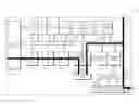
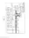
FIG. 3 is a block diagram of a DVB-H receiver according to an exemplary embodiment of the present invention. Referring to FIG. 3, a DVB-H receiver 300 includes a central processing unit (CPU) 301, a general purpose direct memory access (GDMA) unit 303, a bus arbitration and decoding unit 305, a receiving unit 307, a process identifier (PID) filter unit 311, a transport stream (TS) storing unit 313, a dedicated direct memory access (DDMA) unit 315, a memory arbitration and control unit 317, an MPE buffer unit 319, a multi-protocol encapsulation-forward error correction (MPE-FEC) unit 321, a bridge unit 323, a first host interface unit 325, a second host interface unit 327, a peripheral circuit 329, a first bus 340, and a second bus 360.
Transmission data including service data are received by the receiving unit 307. According to the DVB-H standard, the service data are transmitted as TS data. A receiving interface unit 309 performs interfacing between other functional blocks and the receiving unit 307 through the first bus 340. Data received by the receiving unit 300 are transmitted to other functional blocks through the receiving interface unit 309 and the first bus 340.
The CPU 301 and the GDMA unit 303 can be masters of the first bus 340. The bus arbitration and decoding unit 305 receives a bus request from each functional block and performs bus arbitration on the bus requests. The first host interface unit 325 outputs the data stored in the MPE buffer unit 319 to another external device (not shown). A process of storing and processing data in the MPE buffer unit 319 will be described below.
The first bus 340 is connected to the second bus 360 through the bridge unit 323. The peripheral circuit 329 and the second host interface unit 327 can transmit and receive data therebetween through the second bus 360. The peripheral circuit 329 and the second host interface unit 327 can transmit data to and receive data from functional blocks connected to the first bus 340 through the bridge unit 323.
Similar to the first interface unit 325, the second host interface unit 327 outputs data stored in the MPE buffer unit 319 to another external device (not shown). The first interface unit 325 and the second interface unit 327 may include a secure digital input/output (SDIO), a memory interface a serial peripheral interface (SPI), etc. In an exemplary embodiment of the present invention, the first host interface unit 325 may include an SDIO and a memory interface unit. In addition, the second host interface unit 327 may include an SPI.
The operations among the receiving interface unit 309, the CPU 301, the GDMA unit 303, the bus arbitration and decoding unit 305, the first host interface unit 325, the bridge unit 323, the peripheral circuit 3292 and the second host interface unit 327 via the first bus 340 and the second bus 360 are well known to one of ordinary skill in the art to which this exemplary embodiment of the present invention pertains.
As described above, according to an exemplary embodiment of the present invention, a dedicated path for data stored in the MPE buffer unit is used to efficiently perform operations involved with the MPE buffer unit. Referring to the arrows with hatched lines in FIG. 3, a dedicated path for data stored in the MPE buffer unit 319 extends among the receiving unit 307, the PID filter unit 311, the TS storing unit 313, the DDMA unit 315, the memory arbitration and control unit 317, the MPE buffer unit 319, and the MPE-FEC unit 321. Hereinafter exemplary embodiments of the present invention will be described in more detail by focusing on the dedicated path for data stored in the MPE buffer unit 319.
Referring again to FIG. 3, service data received in the receiving unit 307 is transmitted to the PID filter unit 311. Although the following description is provided with the assumption that the received service data is TS data, the present invention is not limited thereto. Service data may be received as ES bursts in the receiving unit 307.
The PID filter 311 filters PID from the received TS data and stores the TS data from which the PID is filtered in the TS storing unit 313. In an exemplary embodiment of the present invention, the TS storing unit 313 may operate in a FIFO (First Input First Output) manner. In addition, the TS storing unit 313 may have a capacity of storing up to five TS data.
The CPU 301 extracts only IP packets by separating a TS header and an MPE header from the TS data stored in the TS storing unit 313. The extracted IP packets are stored in the MPE buffer unit 319. The DDMA unit 315 transmits the TS data from the TS storing unit 313 to the CPU 301 and transmits the IP packets from the CPU 301 to the MPE buffer unit 319. The DDMA unit 315 transmits the data through the above-described dedicated path separated from the first bus. The memory arbitration and control unit 317 performs control and arbitration in response to a connection request to the MPE buffer unit 319.
The MPE-FEC unit 321 performs error correction on the IP packets stored in the MPE buffer unit 319. When the receiving of a single ES burst is completed, the MPE-FEC unit 321 performs error correction on the IP packets stored in the MPE buffer unit 319 in response to a control signal received from the CPU 301. The error-corrected IP packets are stored in the MPE buffer unit 319.
The control signal transmitted from the CPU 301 to the MPE-FEC unit 321 can be an MPE-FEC start signal, a start address on a memory map in the MPE buffer unit 319 that is to be read by the MPE-FEC unit 321, a burst size, etc. The control signal may be transmitted from the CPU 301 to the MPE-FEC unit 321 under the control of a register.
As described above, a control signal, such as an MPE-FEC start signal, a start address, etc., is transmitted from the CPU 301 to the MPE-FEC unit 321, the operations of reading IP packets from the MPE buffer unit 319 and writing the error-corrected IP packets to the MPE buffer unit 319 are performed by the MPE-FEC unit 321.
When an error correction on a single ES burst is completed in the MPE-FEC unit 321, the error-corrected IP packets are transmitted to the first host interface unit 325 and/or the second host interface unit 327. The transmission of the IP packets to the first host interface unit 325 and/or the second host interface unit 327 is performed by the GDMA unit 303. In addition, as described above, the bridge unit 323 is used to transmit the IP packets to the second host interface unit 327.
In an exemplary embodiment of the present invention, in order to cope with multiple services, once a single ES burst (ES1) is received, error correction is performed on the IP packets of the received ES burst (ES1), and simultaneously another consecutive ES burst (ES2) is received, and the IP packets of the ES burst (ES2) are stored in the MPE buffer 319. The operations of performing error correction on the consecutively transmitted ES bursts and storing the IP packets of the ES bursts will be described later with reference to FIGS. 3 through 10.
As described above, in an exemplary embodiment of the present invention, to efficiently process TS data, a dedicated path for the TS data is used. In addition, in order to relieve bottlenecks at the MPE buffer unit 319 which is frequently accessed, access paths to the MPE-FEC unit 321, that is, a path from the DDMA 315, a path from the MPE-FEC unit 321, and a path from the first bus 340, are minimized. In addition, in order to control data congestion occurring when accessing the MPE buffer unit 319, the memory arbitration and control unit 317 arbitrates and controls an access request to the MPE buffer unit 319.
Hereinafter, the operations of correcting errors on consecutively transmitted ES bursts and storing the IP packets of the ES bursts will be described with reference to FIGS. 3 through 10.
FIG. 4 illustrates a situation where consecutive ES bursts are transmitted. When multiple services are provided, the ES bursts can be continuously received during Delta-T without the Off-time, as illustrated in FIG. 4.
As described above, to cope with multiple services, an MPE buffer unit having a memory capacity that is large enough to store the two consecutively received ES bursts is required. In an exemplary embodiment of the present invention, the memory capacity of the MPE buffer unit is minimized using the concept of virtual memory.
In other words, after the IP packets of the first received ES burst (ES1) are stored in the MPE buffer unit 319, the IP packets of the next ES burst (ES2) should be also stored in the MPE buffer unit 319. In addition, after the IP packets of the ES burst (ES1) are stored in the MPE buffer unit 319, the MPE-FEC unit 321 performs error correction on the IP packets of the ES burst (ES1).
The error correction by the MPE-FEC unit 321 is performed at a higher rate than the rate at which the IP packets of the ES burst (ES1) are stored. Accordingly the error correction on the IP packets of the ES burst (ES1) terminates while the IP packets of the ES burst (ES2) are stored. Thus, multiple services can be received by adding a memory capacity that need store only the IP packets of the ES burst (ES2), while the error correction on the IP packets of the ES burst (ES1) is performed, based on the concept of virtual memory.
Compared with the case of receiving a single service, in order to receive multiple services, a memory capacity that is additionally required for the MPE buffer unit 319 should be larger than the product of multiplying the time required to perform error correction on the IP packet of a single ES burst by a maximum bit rate of the ES burst.
According to the DVB-H standard a single ES burst can have a maximum capacity of 2 Mbit. Assuming that the MPE-FEC unit 321 operates at 80 MHz, 2300 system clocks are required to allow the MPE-FEC unit 321 to process data of 2 Mbit. Accordingly, the MPE-FEC unit 321 takes about 28.6 (2300/80 MHz) μs to process an IP packet of 2 MBit.
Assuming that an ES burst according to the DVB-H standard has a maximum bit rate of 16 Mbps, in order to store the IP packet of ES data for 28.6 μs, an additional memory capacity of about 0.458 (28.6 μs*16 Mbps) Mbit is required for the MPE buffer unit 319.
In general, it is desirable to use a memory having a capacity that is slightly greater than the minimum capacity requirement. Accordingly, in the above-described exemplary embodiment, a memory of 0.5 Mbit may be used. In addition, in the DVB-H standard described above, the MPE buffer unit 319 may use an additional memory capacity of 2.5 Mbit, which is the sum of 2 Mbit required to receive a single service and 0.5 Mbit required to receive multiple services according to an exemplary embodiment of the present invention.
In addition, considering that reading and writing can be simultaneously performed on the MPE buffer unit 321, it is not desirable to implement the MPE buffer unit 321 using a single memory. Accordingly, the MPE buffer unit 321 may include a plurality of memories having an additionally required capacity. Specifically, in the above-described embodiment according to the DVB-H standard, the MPE buffer unit 321, which requires an additional memory capacity of 2.5 Mbit, may include five memories each having a capacity of 0.5 Mbit.
Hereinafter, a method according to an exemplary embodiment of the present invention for managing the memory of the MPE buffer unit 321 will be described with reference to FIGS. 5A through 7.
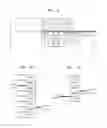
The MPE buffer unit 319 includes a plurality of memory regions MEM0 through MEM4. The plurality of memory regions MEM0 through MEM4 can be separate divided regions in a single memory. It is preferable, however, that the plurality of memory regions MEM0 through MEM4 are physically separate memory regions. In addition each of the physically separate memory regions may be a single port memory. FIG. 5A shows the structures of physical memory regions and virtual memory regions used to store consecutively received ES bursts.
The MPE buffer unit 319 of FIG. 3 includes a plurality of memory regions MEM0 through MEM4. As in the above-described exemplary embodiment, it is also assumed that the memory regions are physically separate single port memory regions and that a single ES burst is stored in four memory regions.
FIG. 5A is provided for explaining the principle of storing consecutively received ES bursts in the MPE buffer unit. Referring to FIG. 5A, in order to store all the consecutively received ES bursts (ES1, ES2), theoretically eight memory regions are required. In FIG. 5A, lower unhatched blocks correspond to physical memory regions, and upper hatched blocks correspond to virtual memory regions.
In FIG. 5A, there are physically five memory regions. The memory map, however, seems to have eight memory regions. In other words, the MPE buffer unit may operate as if it includes eight memory regions. Actually, however, mirrors of memory regions MIR_MEMO through MIR_MEM2 in the virtual memory region in FIG. 5A are located in another memory map. In FIG. 5A, from “0x200—000”, which is a base address, to “0x204_FFFF” are mapped to five memories MEM0 through MEM4. From “0x205—0000” to “0x207_FFFF”, however, are mapped to mirrors of the memories MEM0 through MEM2 in another memory map.
FIG. 5A is provided for explaining start addresses of consecutively received ES bursts. When consecutive ES bursts (ES1 through ES5) are received as in FIG. 4, the physical start address of the ES burst (ES1) is the base address, that is, “0x200—0000”.
When memory mapping is achieved as in FIG. 5A, the physical start address of the ES burst (ES2) will be “base address+4—0000”, the physical start address of the ES burst (ES3) will be “base address+3—0000”, the physical start address of the ES burst (ES4) will be “base address+2—0000”, and the physical start address of the ES burst (ES5) will be “base address+1—0000”. The start addresses of consecutively received ES bursts are determined in this manner.
As described above, the data actually stored in the MPE buffer unit 319 are the IP packets included in the ES bursts. After all the IP packets included in the ES bursts are stored in the MPE buffer unit 319, the MPE-FEC unit 321 receives a control signal including the start address of each IP packet stored in the MPE buffer unit 319 from the CPU 301, reads an IP packet stored in the MPE buffer unit 319 in response to the control signal, and performs error correction on the IP packet. For reference, the error-corrected IP packet is stored in the same region of the MPE buffer unit 319 as where the IP packet was stored before being error-corrected.
As described above, even when consecutive ES bursts are received, the start addresses of the IP packets of the ES bursts stored in the MPE buffer unit 319 can be identified. Thus, the MPE-FEC unit 321 can read data, that is, IP packets, corresponding to consecutive addresses, without erroneously accessing a boundary between memory regions or without occurrence of a wrap around.
For example, in a receiver that can receive two services, ES bursts (ES1 and ES2) are consecutively received. Accordingly, memories MEM0 through MEM3 are used for the ES burst (ES1), and memory MEM4 and mirror memory regions MIRR_MEM0 through MIRR_MEM2 are used for the ES burst (ES2).
More specifically, after the IP packets included in the ES burst (ES1) are stored in the memory regions MEM0 through MEM3, some of the IP packets included in the ES burst (ES2) are stored in the memory MEM4, while error correction is performed on the IP packets of the ES burst (ES1) stored in the memories MEM0 through MEM3.
After error correction on the IP packets of the ES burst (ES1) stored in the memories MEM0 through memory MEM3 is completed, the error-corrected IP packets of the ES burst (ES1) stored in the memory regions MEM0 through MEM3 are output to an external host (not shown), and thus, the memory regions MEM0 through MEM3 are sequentially emptied. The remaining IP packets in the ES burst (ES2) are sequentially stored in the memory regions MEM0 through MEM2.
As described above, in the exemplary embodiment of the present invention based on the concept of virtual memory, the MPE buffer unit 321, which actually includes only five memory regions, operates as if there are eight memory regions using software. Thus, access to the MPE buffer unit 321 should be controlled not to induce unwanted over-writing in the MPE buffer unit 321.
Thus, in order to prevent the IP packets of an ES burst consecutively received before the error-corrected IP packets are output to the external host from being written to the MPE buffer unit 319, a data transmission rate of a host interface through which the error-corrected IP packets are output should be higher than the IP packet input rate of the ES burst.
In the DVB-H receiver of FIG. 3, the second host interface 327 may include an SPI. In this case, the SPI may support a maximum rate of 32 Mbps. In addition, the first host interface unit 327 may include an SDIO or a memory interface. The transmission rate of the SDIO or the memory interface is greater than the transmission rate of the serial peripheral interface (SPI).
As described above, in the exemplary embodiments of the present invention, the outputting of the error-corrected IP packets to the external host can be achieved simultaneously with the storing of the IP packets of consecutively received ES bursts in the MPE buffer unit 319. Accordingly, it is preferred that the MPE buffer unit 319 is implemented with five separate memories, rather than the five memory regions of the MPE buffer unit 319 being implemented in a single memory.
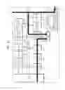
FIG. 6 is a diagram for explaining the operation of the circuit in FIG. 3 when consecutive ES bursts are received.
Referring to FIG. 6, the IP packets of the ES burst (ES1) received during the interval between T0 and T1 are stored in the memories MEM0 through MEM3. Next, error correction is performed on the IP packets of the ES burst (ES1) stored in the memories MEM0 through MEM3 during the interval between the T1 and T2 and the IP packets of the consecutively received ES burst (ES2) are stored in the memory MEM4.
After the error correction on the IP packets of the ES burst (ES1) stored in the memories MEM0 through MEM3 is completed, in the interval between T2 and T1, the MPE buffer unit 319 reads the error-corrected IP packets of the ES burst (ES1), which will be transmitted to the external host, from the MPE buffer unit 319 in the interval between T2 and T3, and simultaneously write the IP packets of the consecutively received ES burst (ES2) to the MPE buffer unit 319?. Accordingly, the memory arbitration and control unit 317 should arbitrate accesses to the MPE buffer unit 319 for the reading and writing operations.
The DDMA 315 accesses the MPE buffer unit 319 to write the IP packets of the consecutively received ES burst thereto. In addition, since the data stored in the MPE buffer unit 319 are transmitted to the external host via the first bus 340 or the second bus 360, the GDMA 303 accesses the MPE buffer unit 319 to read the data stored therein. In order to prevent unwanted over-writing to the MPE buffer unit 319, the error-corrected IP packets stored in the MPE buffer unit 319 have to be transmitted to the external host before the IP packets of the consecutively received ES burst are stored in the MPE buffer unit 319.
Accordingly, in an exemplary embodiment of the present invention, a higher priority is granted to the GDMA unit 303 than to the DDMA unit 315 to allow the error-corrected IP packets stored in the MPE buffer unit 319 to be transmitted to the external host before the IP packets of the consecutively received ES burst are stored in the MPE buffer unit 319.
In addition, the MPE-FEC unit 321 may also request an access to the MPE buffer unit 319. For example, while the MPE-FEC unit 21 accesses the memory regions of the MPE buffer unit 319 in which the IP packets of the ES burst (ES1) are stored, the DDMA unit 315 accesses the remaining memory regions. In addition, since the GDMA unit 303 transmits data to the external host after the error correction by the MPE-FEC unit 321 is completed, it is unlikely that the MPE-FEC unit 321 and the DDMA unit 315 or the GDMA 303 simultaneously request access to the same memory region. In other words, it is unlikely that an access request by the MPE-FEC unit 321 an access request by the DDMA unit 315 or the GDMA unit 303 collides. In an exemplary embodiment of the present invention, however, a higher priority is granted to an access request by the DDMA unit 315 than to an access request by the MPE-FEC unit 321 only for the purpose of arbitrating the priorities of access requests.
In general, the TS storing unit 313, and the SPIs included in the host interface unit, operates according to a FIFO method. The TS storing unit 313 can store up to five TSs, while an SPI has a very small capacity of, in general, 4 bytes, or 12 bytes at maximum. This is another reason why granting a higher priority to the access request by the GDMA unit 303 than to the access request by the DDMA unit 315 in addition to the above-described reason for preventing over-writing to the MPE buffer unit 319.
In addition, in an embodiment of the present invention, because the DDMA unit 315 uses a dedicated path for the TS data of IP packets of the ES bursts, when a wait signal WAIT (refer to FIG. 8) is not received from the memory arbitration and control unit 317, the DDMA unit 315 accesses the MPE buffer unit 319 at a high transmission rate through the dedicated path. In an exemplary embodiment of the present invention, when the wait signal WAIT is not received, the DDMA unit 315 may access the MPE buffer unit 321 at a maximum transmission rate of 640 Mbps (80 Mhz×8 bit).
In addition, the memory arbitration and control unit 317 arbitrate access requests to the MPE buffer unit 319 when an access request by the DDMA unit 315 to allow writing and an access request by the GDMA unit 303 to allow reading both request access to the same memory region of the MPE buffer unit 319.
As described above, since the rate at which the IP packets are output from the MPE buffer unit 319 to the external host is higher than the rate at which the IP packets of the ES bursts are input to the MPE buffer unit 319, after a certain period of time passes, an access request by the DDMA unit 315 for writing and an access request by the GDMA unit 303 for reading occur in different memory regions. In the above-described exemplary embodiment of the present invention, since the plurality of memory regions MEM0 through MEM4 are physically separate single port memories, there is no need for the memory arbitration and control unit 317 to arbitrate the access request by the DDMA unit 315 and the access request by the GDMA unit 303. In other words, by implementing the plurality of memory regions with physically separate single port memories, intervals in which the arbitration of the memory arbitration and control unit 317 are required can be minimized.
FIGS. 7A and 78 are diagrams for explaining the operation of managing the memory in the interval between T2 and T3 in FIG. 6, using a software concept, FIG. 7A, and a hardware concept FIG. 7B.
Assuming that two ES bursts (ES1 and ES2) are consecutively received, and four memory regions are required to store the IP packets of a single ES burst, a total of eight memory regions are required when using the software concept. Referring to FIGS. 6, 7A and 78, in the interval between T0 and T1 the IP packets of the ES burst (ES1) are stored in the memory regions MEM0 through MEM3. In the interval between T1 and T2, error correction is performed on the IP packets stored in the memory regions MEM0 through MEM3, and the IP packets of the consecutively received ES burst (ES2) are stored in the memory region (MEM4).
In the interval between T2 and T2, after the error correction of the IP packets stored in the memory regions (MEM0 through MEM3) is completed, it is likely that the DDMA unit 315 and the GDMA unit 303 request respective access to the same physical memory region. Thus, arbitration by the memory arbitration and control unit 317 is required.
FIGS. 7A and 7B are diagrams for explaining the operation of the memory arbitration and control unit 317. In FIG. 8, the arrows with hatched lines denote paths for transmitting data, that is, IP packets. Referring to FIGS. 6 through 8, at T2 at which the error correction on the IP packets of the ES burst (ES1) stored in the memory regions MEM0 through MEM3 is completed, the GDMA unit 303 transmits an access request (RD REQ) to allow reading the error-corrected IP packets stored in the memory regions MEM0 through MEM3.
Since the IP packets of the ES burst (ES2) are consecutively written to the MPE buffer unit 319 after T1, the DDMA unit 315 also transmits an access request for writing (WR REQ) at T2 in order to write the IP packets to the MPE buffer unit 319.
While the IP packets of the ES burst (ES2) are stored in the memory region (MEM4) in the interval between T1 and T2, the IP packets of the ES burst (ES2) should be stored in the mirror memory region (MIR_MEM0) with an address of “0x205—0000” after T2. Accordingly, after T2, the DDMA unit 315 transmits an access request (WR REQ) to allow writing to the memory region MEM0.
In order to prevent over-writing to the MPE buffer unit 319, the GDMA unit 303 sequentially read the IP packets stored in the memory regions MEM0 through MEM3, and the GDMA 303 transmits an access request (RD REQ) to allow reading from the memory region MEM0 at T2.
In addition, the duration for which the MPE-FEC unit 321 performs error correction is shorter than the duration for which the IP packets of the ES burst (ES2) are stored in the memory region MEM4. Thus, an access request (WR REQ) by the DDMA unit 315 and an access request by the GDMA unit 303 collide at or after T2. In other words, the access request (WR REQ) by the DDMA unit 315 and the access request by the GDMA unit 303 collide at least in the interval between T2 and T3.
In an exemplary embodiment of the present invention, when the access request (WE REQ) by the DDMA unit 315 and the access request by the GDMA unit 303 collide, a priority is granted to the access request by the GDMA unit 303. In other words, when the access request (WR REQ) by the DDMA unit 315 to allow writing to the memory region MEM0 and the access request by the GDMA unit 303 to allow writing to the memory region MEM0 collide at or after T2, the memory arbitration and control unit 218 transmits a wait signal WAIT to the DDMA unit 315 and grants a priority to the access request by the GDMA unit 303 to allow the GDMA unit 303 to access the MPE buffer unit 319.
Accordingly, after all the error-corrected IP packets of the ES burst (ES1) stored in the memory region MEM0 are transmitted to the external host, the IP packets of the ES burst (ES2) are stored in the memory region MEM0. The error-corrected IP packets of the ES burst (ES1) stored in the memory region MEM1 are transmitted to the external host while the IP packets of the ES burst (ES2) are stored in the memory region (MEM0).
As described above, in an exemplary embodiment of the present invention, since the transmission rate of the host interface is faster than the receiving rate of the ES bursts, once the access request (WR REQ) by the DDMA unit 315 and the access request by the GDMA unit 303, both of which request access to the memory region MEM0, are arbitrated, an access request (WR REQ) by the DDMA unit 315 and an access request by the GDAM unit 303, both of which request access to the same memory region, do not collide.
As illustrated in FIGS. 7A and 7B, after the access requests to the memory region MEM0 are arbitrated, the error-corrected IP packets of the ES burst (ES1) stored in the memory region MEM2 are output to the external host while the IP packets of the ES burst (ES2) are written to the memory region MEM1. In other words, respective access to the MPE buffer unit 319 by the DDMA unit 315 and the GDMA unit 303 can be efficiently controlled using a software concept, as illustrated in FIG. 7A, and using a hardware concept, as illustrated in FIG. 7B.
Although it is assumed above that the transmission rate of the host interface is greater than the ES burst receiving rate, it is obvious to one of ordinary skill in the art that memory can be efficiently managed by arbitrating access requests to the same memory region using the memory arbitration and control unit 317 even when the transmission rate of the host interface is slower than the ES burst receiving rate.
FIG. 8 illustrates the case where the memory arbitration and control unit 317 transmits a wait signal WAIT to the MPE-FEC unit 321 or the GDMA unit 303, and in particular, to the first bus 340. As described above, however, the collision of the access request (RD/WR REQ) by the MPE-FEC unit 321 and the access request by the DDMA unit 315 or the GDMA unit 303, which both request access to the same memory region, does not occur in the interval between T2 and T3. Thus, a wait signal WAIT is not transmitted to the MPE-FEC unit 321 in the interval between T2 and T3.
Even when the access request (WR REQ) by the DDMA unit 315 and the access request by the GDMA unit 303 collide, a wait signal WAIT is not transmitted to the GDMA unit 303 in the interval between T2 and T3 because a priority is granted to the access request by the GDMA unit 303.
Referring to FIG. 6, all the error-corrected IP packets of the ES burst (ES1) stored in the MPE buffer unit 319 are output to the external host at T3. Accordingly, the IP packets of the ES burst (ES2) are stored in the memory regions MEM4 and MEM0 through MEM2 in the interval between T3 and T4.
All the IP packets of the ES burst (ES2) are stored in the MPE buffer unit 319 at T14, and error correction is performed on the IP packets of the ES burst (ES2) stored in the MOE buffer unit 319 in the interval between T4 and T5. Finally, after the error correction on the IP packets of the ES burst (ES2) is completed at T5, the error-corrected IP packets of the ES burst (ES2) stored in the MPE buffer unit 319 are output to the external host in the interval between T5 and T6.
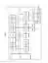
FIG. 9 is a timing diagram for explaining the operation of a DVB-H receiver according to an exemplary embodiment of the present invention. In FIG. 9 CLK denotes a system clock of 80 MHz, for example.
RDREQ_GDMA denotes an access request issued by the GDMA unit 303 to allow reading data from the MPE buffer unit 319. DATARD_GDMA represents a data, that is, IP packets, read operation from MPE buffer unit 319 by the GDMA unit 303, that is, the operation of the GDMA unit 303 of transmitting IP packets from the MPE buffer unit 319 to the external host. As is apparent from DATARD_GDMA in FIG. 9, the GDMA unit 303 regularly transmit IP packets by one word. In an exemplary embodiment of the present invention, since a top priority is granted to the GDMA unit 303, when the GDMA unit 303 requests an access, the GDMA unit 303 can immediately access the MPE buffer unit 319.
In addition, in FIG. 9, WRREQ_DDMA denotes an access request issued by the DDMA unit 315 to write data to the MPE buffer unit 319, and WAIT_ARS_DDMA denotes a wait signal transmitted from the memory arbitration and control unit 317 to the DDMA unit 315. DATAWR_DDMA denotes the operation of writing data, that is, IP packets, to the MPE buffer unit 319 by the DDMA unit 315.
As is apparent from DATAWR_DDMA in FIG. 9, since a dedicated path for transmitting TS data or IP packets included in ES bursts is used in an exemplary embodiment of the present invention, the DDMA unit 315 can transmit data in bursts via the dedicated path at a high rate.
As described above, in an exemplary embodiment of the present invention, by granting a higher priority to the GDMA unit 303 than to the DDMA unit 315, over-writing to the MPE buffer unit 319 is prevented. In this regard, referring to FIG. 9, when an access request by the DDMA unit 315 and an access request by the GDMA unit 303 collide, the memory arbitration and control unit grants a priority to the GDMA unit 303 to allow the GDMA unit 303 to immediately access the MPE buffer unit 319 and read data therefrom. Meanwhile, the memory arbitration and control unit 317 outputs a wait signal WAIT to the DDMA unit 315, and access of the DDMA unit 315 to the MPE buffer unit 319 is restricted while the DDMA unit 315 receives the wait signal WAIT. According to an exemplary embodiment of the present invention, however, since the DDMA unit 315 uses a dedicated path for TS data or IP packet, the DDMA unit 315 can transmit all IP packets in a sufficient time without being greatly affected by the wait signal WAIT that is occasionally generated.
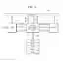
FIG. 10 is a block diagram of a receiver according to an exemplary embodiment of the present invention for explaining the flow of data in the interval between T1 and T2 of FIG. 6. FIG. 11 is a block diagram of a receiver according to an exemplary embodiment of the present invention for explaining the flow of data in the interval between T2 and T3.
As described above, the MPE-FEC unit 321 performs error correction on the IP packets of the ES burst (ES1) stored in the MPE buffer unit 319, and the IP packets of the consecutively received ES burst (ES2) are stored in the MPE buffer unit 319.
Accordingly, in the interval between T1 and T2, the TS data or IP packets of the ES burst (ES3) input to the receiver 300 are stored in the MPE buffer unit 319 via the receiving unit 307, the PID filter unit 311, the TS storing unit 313, the DDMA unit 315, and the memory arbitration and control unit 317. On the other hand, the MPE-FEC unit 321 performs error correction on the data, that is, IP packets of the ES burst (ES1) stored in the MPE buffer unit 319 in the interval between T1 and T2. Accordingly, the data, that is, IP packets, of the ES burst (ES1) are transmitted and received through the path between the MPE-FEC unit 321 and the MPE buffer unit 319 (refer to FIG. 10).
On the other hand, the error-corrected IP packets of the ES burst (ES1) stored in the MPE buffer unit 319 are transmitted to the external host through the first bus 340 and/or the second bus 360 in the interval between T2 and T3, and the IP packets of the consecutively received ES burst (ES2) are sequentially stored in the MPE buyer unit 319.
Thus, the path of the data of the ES burst (ES2) in the interval between T2 and T3 is the same as the path of the data of the ES burst (ES2) in the interval between T1 and T2. In addition, the IP packets of the ES burst (ES1) stored in the MPE buffer unit 319 in the interval between T2 and T3 are transmitted to the external host through a path including the first bus 340 and the first host interface unit 325 or a path including the first bus 340, the bridge unit 323, the second bus 360, and the second host interface unit 327 (refer to FIG. 11).
As described above, a receiver according to an exemplary embodiment of the present invention can effectively process consecutively received elementary streams using a minimum capacity of MPE buffer memory. A receiver according to an exemplary embodiment of the present invention can include a minimum capacity of an on-chip MPE buffer memory, which is integrated into a chip of the receiver, and can cope with multiple service.
In a receiver according to an exemplary embodiment of the present invention, a main data path is formed using a dedicated bus, separated from a general-purpose bus, such as an AMBA bus, so that an MPE buffer that data are frequently input to and output from can be effectively controlled. Accordingly, a memory map of the receiver can be freely designed regardless of software and hardware requirement. The DVB-H receiver according to an exemplary embodiment of the present invention can be designed to be compact and is suitable for portable devices such as mobile phones.
While the present invention has been particularly shown and described with reference to exemplary embodiments thereof, it will be understood by those of ordinary skill in the art that various changes in form and details may be made therein without departing from the spirit and scope of the present invention as defined by the following claims.
Claims
What is claimed is:1. A method of consecutively receiving input burst data, the method comprising:
storing data in a first format of current burst data in predetermined regions of a buffer, wherein the predetermined regions constitute less than all of the buffer regions; and
performing error correction on the data in the first format of the current burst data after all the data in the first format is stored and simultaneously storing some data in the first format of next burst data in remaining regions of the buffer.
2. The method of claim 1, after performing the error correction on the data in the first format of the current burst data, further comprising outputting the error-corrected data in the first format and storing the data in the first format of the next burst data in the predetermined regions of the buffer that are empty as a result of the error-corrected data in the first format being output therefrom.
3. The method of claim 1 further comprising forming the buffer as a plurality of physically separate memory regions, and forming the remaining regions of the buffer in which some data in the first format of the next burst data are stored as at least one physically separate sub-memory.
4. The method of claim 3, further comprising forming each of the plurality of physically separate sub-memories as a single port memory.
5. The method of claim 3, further comprising forming each of the plurality of sub-memories with a memory capacity that is at least larger than a product of multiplying a time required to perform the error correction by a maximum bit rate of the burst data.
6. The method of claim 2, further comprising outputting the error-corrected data in the first format at a rate that is greater than a rate at which the burst data are received.
7. The method of claim 1, complying with the DVB-H standard.
8. The method of claim 1, wherein the burst data includes elementary stream (ES) bursts, and the data in the first format includes IP packets.
9. A receiver comprising:
a buffer unit that includes a plurality of memory regions and that stores consecutively received burst data in a first format;
an error correction unit that performs error correction on the burst data in the first format;
an access unit that accesses the buffer unit to allow writing the data in the first format of the received burst data; and
a buffer arbitration unit that arbitrates access requests to the buffer unit,
wherein the access unit allows the data in the first format to be stored in the buffer unit through a dedicated access path.
10. The receiver of claim 9, wherein the access unit allows all the data in the first format of current burst data to be stored in predetermined memory regions of the buffer unit, wherein the predetermined regions constitute less than all of the buffer unit and some data in the first format of next burst data to be stored in remaining memory regions of the buffer unit.
11. The receiver of claim 10, wherein the error correction unit performs error correction on the data in the first format of the current burst data while some data in the first format of the next burst data are stored in the remaining memory regions of the buffer unit after all the data in the first format of the current burst data are stored in the predetermined memory regions of the buffer unit.
12. The receiver of claim 11 wherein, after the error correction on the data in the first format of the current burst data is completed, the error-corrected data in the first format are output to an external host, and the data in the first format of the next burst data are stored in the predetermined memory regions of the buffer unit that are empty as a result of the error-corrected data in the first format being output to the external host.
13. The receiver of claim 12, wherein, when an access request to allow outputting data to the external host and an access request to allow storing the data in the first format both request access to the same memory region in the buffer unit are received the memory arbitrate unit arbitrates the access requests so that the access request to allow outputting data to the external host is accepted prior to the access request to allow storing the data in the first format.
14. The receiver of claim 12, wherein an access request to allow outputting data to the external host and an access request to allow storing the data in the first format request access to different memory regions in the buffer unit are separately accepted.
15. The receiver of claim 9, wherein the plurality of memory regions are physically separate memory regions.
16. The receiver of claim 15, wherein each of the plurality of memory regions is a single port memory.
17. The receiver of claim 9, further comprising:
a process identifier filter unit that generates data in a second format by filtering process identifiers in the burst data; and
a storing unit that stores the data in the second format.
18. The receiver of claim 17, wherein the access unit receives the data in the second format through a dedicated path including the process identifier filter unit and the storing unit.
19. The receiver of claim 17, wherein the data in the second format comprise transport stream data.
20. The receiver of claim 9, wherein the receiver complies with the DVB-H standard.
21. The receiver of claim 9, wherein the burst data includes elementary stream bursts, and the data in the first format includes internet protocol packets.
Images & Drawings included:


Sources:
- United States Patent and Trademark Office - verify current appl. status at the USPTO↗
Similar patent applications:
Recent applications in this class:
- » 20240292771 2024-08-29
Campanula plant named 'Twilight' - » 20240251691 2024-07-25
HYDRANGEA PLANT NAMED 'HYLV17520' - » 20240251690 2024-07-25
Vaccinium Plant Named 'BWPBLUE02' - » 20240251689 2024-07-25
BLUEBERRY PLANT NAMED 'FC13-113' - » 20240251688 2024-07-25
BLUEBERRY PLANT NAMED 'FCM14-057' - » 20240237567 2024-07-11
PONGAMIA VARIETIES - » 20240224827 2024-07-04
PELARGONIUM PLANT NAMED 'PEQZ0103' - » 20240215470 2024-06-27
Agapanthus plant named 'Monsapho' - » 20240215469 2024-06-27
plant named ‘LOCORA3519’ - » 20240206359 2024-06-20
CORYLUS PLANT NAMED 'BWM01'