Method for manufacturing leads
US20080106877A1
2008-05-08
11/979,487
2007-11-05
✅ Patent granted
US 8,196,291 B2
2012-06-12
-
-
Carl Arbes
2030-12-13
Abstract:
A system method for manufacturing leads is provided. The method includes providing a conductive sheet, shaping the conductive sheet into at least two opposing longitudinal strips and a plurality of interposing strips, masking lateral sides and a center of the plurality of interposing strips, covering the exposed surface with a conductor and severing the conductive sheet at least along center mask. The plurality of interposing strips are preferably flexible and configurable into desired shapes for potential future attachment to an integrated circuit.
Assignee:
- General Dynamics Advanced Information Systems, Inc 54 🇺🇸 Fairfax, VA, United States
Interested in similar patents?
Get notified when new applications in this technology area are published.
Classification:
H05K3/3426 » CPC main
Apparatus or processes for manufacturing printed circuits; Assembling printed circuits with electric components, e.g. with resistor electrically connecting electric components or wires to printed circuits by soldering; Surface mounted components; Leaded components characterised by the leads
H01L21/4821 » CPC further
Processes or apparatus adapted for the manufacture or treatment of semiconductor or solid state devices or of parts thereof; Manufacture or treatment of semiconductor devices or of parts thereof the devices having at least one potential-jump barrier or surface barrier, e.g. PN junction, depletion layer or carrier concentration layer; Manufacture or treatment of parts, e.g. containers, prior to assembly of the devices, using processes not provided for in a single one of the subgroups -; Conductive parts Flat leads, e.g. lead frames with or without insulating supports
H01R43/16 » CPC further
Apparatus or processes specially adapted for manufacturing, assembling, maintaining, or repairing of line connectors or current collectors or for joining electric conductors for manufacturing contact members, e.g. by punching and by bending
H05K2201/10689 » CPC further
Indexing scheme relating to printed circuits covered by; Details of components or other objects attached to or integrated in a printed circuit board; Details of electrical connections of non-printed components, e.g. special leads; Components characterised by their electrical contacts Leaded Integrated Circuit [IC] package, e.g. dual-in-line [DIL]
H05K2201/10757 » CPC further
Indexing scheme relating to printed circuits covered by; Details of components or other objects attached to or integrated in a printed circuit board; Details of electrical connections of non-printed components, e.g. special leads; Details of leads; Shape details Bent leads
H05K2201/10946 » CPC further
Indexing scheme relating to printed circuits covered by; Details of components or other objects attached to or integrated in a printed circuit board; Details of electrical connections of non-printed components, e.g. special leads; Details of leads; Other details Leads attached onto leadless component after manufacturing the component
Y02P70/50 » CPC further
Climate change mitigation technologies in the production process for final industrial or consumer products Manufacturing or production processes characterised by the final manufactured product
Y02P70/50 » CPC further
Climate change mitigation technologies in the production process for final industrial or consumer products Manufacturing or production processes characterised by the final manufactured product
Y10T29/49117 » CPC further
Metal working; Method of mechanical manufacture; Electrical device making Conductor or circuit manufacturing
Y10T29/49121 » CPC further
Metal working; Method of mechanical manufacture; Electrical device making; Conductor or circuit manufacturing Beam lead frame or beam lead device
Y10T29/4913 » CPC further
Metal working; Method of mechanical manufacture; Electrical device making; Conductor or circuit manufacturing; On flat or curved insulated base, e.g., printed circuit, etc. Assembling to base an electrical component, e.g., capacitor, etc.
H01L23/495 IPC
Details of semiconductor or other solid state devices; Arrangements for conducting electric current to or from the solid state body in operation, e.g. leads, terminal arrangements ; Selection of materials therefor consisting of soldered constructions Lead-frames or other flat leads
H05K1/14 IPC
Printed circuits; Details Structural association of two or more printed circuits
H05K1/14 IPC
Printed circuits; Details Structural association of two or more printed circuits
H05K3/36 IPC
Apparatus or processes for manufacturing printed circuits Assembling printed circuits with other printed circuits
H05K3/36 IPC
Apparatus or processes for manufacturing printed circuits Assembling printed circuits with other printed circuits
H01R43/00 IPC
Apparatus or processes specially adapted for manufacturing, assembling, maintaining, or repairing of line connectors or current collectors or for joining electric conductors
Description
CROSS REFERENCE TO RELATED APPLICATIONSThe instant application claims priority to U.S. Provisional Application No. 60/856,813, filed Nov. 6, 2006, the disclosure of which in hereby incorporated by reference in its entirety.
BACKGROUND OF THE INVENTION1. Field of the Invention
The present invention relates to shaped leads, preferably C-shaped leads. More specifically, the present invention relates to systems and methods for manufacturing C-shaped leads for miniature leadless components and/or the assembly of Printed Circuit Board (PCB) for miniature leadless components that use such leads.
2. Discussion of Background Information
The current generation of leadless components has relatively small solder pads (˜0.008 inch—almost twice the thickness of human hair) and small pitch (0.020 inch—almost six times the thickness of human hair). These components typically have relatively lower thermal coefficients of expansion (TCE) than high density boards. Typical solder joints may be acceptable for commercial electronics with low life expectancy of at the most three years, and will therefore not meet 20-year durability requirements of military electronics used in harsh environments.
Shaped leads, particularly C-shaped leads, formed through traditional punch press methodologies are not viable for solder pads of this size due to the size and the softness of pure copper foil.
SUMMARY OF THE INVENTIONAccording to an embodiment of the invention, a method for manufacturing leads is provided. The method includes providing a conductive sheet, shaping the conductive sheet into at least two opposing longitudinal strips and a plurality of interposing strips, masking lateral sides and a center of the plurality of interposing strips, covering the exposed surface with a conductor and severing the conductive sheet at least along center mask. The plurality of interposing strips are preferably flexible and configurable into desired shapes for potential future attachment to an integrated circuit.
The above-embodiment may have various optional features. For at least one of the severed sections of conductive sheet, the method may also include bending the plurality of interposing strips to form the desired shaped leads, attaching one side of the leads to an integrated circuit, removing the lateral side of the conductive strip, and attaching the other side of the leads to a support. The bending may comprises folding the interposing strips such that the lateral mask is aligned with the center mask. The shaping may comprise etching. The masking may comprise applying a solder mask. The covering may comprises plating. The severing may comprise cutting the conductive sheet approximately down the center of the central mask, wherein the conductive strip is thereby separated into roughly equal sections. The providing may comprises providing a copper-based foil sheet approximately 2-10 mils thick.
According to another embodiment of the invention, a method for manufacturing leads is provided. The method includes providing a conductive sheet in a substantially ladder-shaped pattern, including two lateral supports and a plurality of rungs, applying solder mask on the rungs adjacent to lateral supports and down the center of the rungs to form a center mask and two lateral masks, plating exposed portions of the masked conductive sheet with a conductor; and splitting the conductive sheet down the center mask to form two sections. The plurality of split rungs are preferably flexible and configurable into desired shapes for potential future attachment to an integrated circuit.
The above embodiment may have various optional features. For at least one of the severed sections of conductive sheet, the method may include bending the plurality of interposing strips to form the desired shaped leads, attaching one side of the leads to an integrated circuit, removing the lateral side of the conductive strip, and attaching the other side of the leads to a support. The bending may comprise folding the interposing strips such that the lateral mask is aligned with the center mask. The shaping may comprise etching. The masking may comprise applying a solder mask. The covering may comprises plating. The severing may comprise cutting the conductive sheet approximately down the center of the central mask, wherein the conductive strip is thereby separated into roughly equal sections. The providing may comprises providing a copper-based foil sheet approximately 2-10 mils thick. The center mask may be approximately twice the width of the lateral masks.
According to yet another embodiment of the invention, a method for manufacturing an integrated circuit, is provided. The method includes providing a conductive sheet, etching the conductive sheet to define at least two opposing longitudinal strips and a plurality of interposing strips, applying a mask to lateral sides and a center of the plurality of interposing strips, and severing the conductive sheet at least along the center mask to define separate sections. For at least a portion of one the separate portions, the method also includes bending the plurality of interposing strips to form the desired shaped leads, attaching one side of the leads to an integrated circuit, and removing the lateral side of the conductive strip. The method may further include attaching the other side of the leads to a printed wiring board.
According to yet another embodiment of the invention, an integrated circuit is provided. A plurality of flexible copper-based leads have first and second strips of solder mask. The plurality of leads are folded to define substantially a C-shape, wherein the first and second strips of solder mask are substantially aligned and facing each other inside the C-shape. One side of the outer portion of the C-shape is in electrical contact with the integrated circuit. The other side of the outer portion of the C-shape is configured for electrical contact with another electrical element. The another electrical element may be a printed wiring board.
Other exemplary embodiments and advantages of the present invention may be ascertained by reviewing the present disclosure and the accompanying drawings.
BRIEF DESCRIPTION OF THE DRAWINGSThe present invention is further described in the detailed description which follows, in reference to the noted plurality of drawings by way of non-limiting examples of certain embodiments of the present invention, in which like numerals represent like elements throughout the several views of the drawings, and wherein:
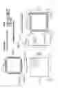
FIG. 1 shows various views of an embodiment of the invention with preferred dimensions;
FIGS. 2(a)-2(e) show various production steps of an embodiment of the invention for producing a strip of leads; and
FIGS. 3(a)-3(c) show various production steps of an embodiment of the invention for attaching a strip of leads.
DETAILED DESCRIPTION OF THE EXEMPLARY EMBODIMENTThe particulars shown herein are by way of example and for purposes of illustrative discussion of the embodiments of the present invention only and are presented in the cause of providing what is believed to be the most useful and readily understood description of the principles and conceptual aspects of the present invention. In this regard, no attempt is made to show structural details of the present invention in more detail than is necessary for the fundamental understanding of the present invention, the description taken with the drawings making apparent to those skilled in the art how the several forms of the present invention may be embodied in practice.
Examples of miniature leadless components along with associated dimensions are shown in FIG. 1. Embodiments of the present invention are directed to providing C-leads for such components. However, the invention is not so limited, and other applications for the leads and other shapes (e.g., S or Z) can also be used.
Referring now to FIG. 2(a), a metal sheet 202 is provided, preferably made of copper-based materials such as pure copper foil or beryllium copper alloy foil. Sheet 202 is preferably 2-10 mils thick, particularly approximately 5 mils thick. Each sheet 202 defines a frame in a larger sheet (not shown) that measures 18 inches by 24 inches, although any desired dimensions could be used. Each sheet 202 has four holes 204 for alignment and/or mounting purposes, although any number of holes, shapes, and/or alignment methodologies may be used. Each sheet preferably provides approximately 200 leads or lead frames.
Referring now to FIG. 2(b), a “ladder” pattern is etched into the sheet 202 using standard etching methodologies. The width of the ladder arms 206 is preferably 50-70 mils, particularly 60 mils. Each rung 208 is preferably 3-15 mils wide, particularly approximately 7 or 10 mils. Each rung is separated by gaps of approximately 5-10 mils. Other dimensions could be used based upon the layout of leadless contacts on the chip for which the leads are ultimately intended.
Referring now to FIG. 2(c), a solder mask is applied to sheet 202 to form a top, bottom, and center section 210, 212, and 214. Center section 212 is preferably approximately twice as wide as top and bottom sections 210 and 214. The solder mask is preferably 2-4 mils, approximately 3 mils thick, made of a dry film such as that available from DUPONT®. An appropriate thickness and/or type of mask material may be used as appropriate for the application.
Referring now to FIG. 2(d), the exposed copper is plated with metal. Tin, immersion silver, electroless-nickel-immersion-gold (ENIG) and nickel alloys are non-limiting examples of appropriate metals, although other metals and/or alloys could be used. The plating prevents corrosion and oxidation of the underlying copper from soldering.
Referring now to FIG. 2(e), the sheet 202 is cut approximately in half along its longitudinal axis 216 (between the arms 206) to define two halves 218 and 220. Both halves can now be processed in the same way, so further reference will be made to only one of the halves.
Referring now to FIG. 3(a), C-unit 300 (corresponding to 218 or 220 in FIG. 2(e)) is formed by moving the remaining portion of center section 214. The solder mask holds the leads in place during subsequent soldering.
Referring now to FIG. 3(b), the exposed upper surface of C-unit 300 is soldered as appropriate to a leadless chip 302. Any excess portion of C-unit 300 which extends beyond unit 302 (including the former ladder arm 206) can be trimmed through known techniques. Referring now to FIG. 3(c), the exposed lower surface of C-unit 300 is soldered to a printed wiring board 304. This completes the installation.
C-leads manufactured using the above technique have an inherent compliancy from the soft copper. This accommodates any difference in thermal coefficients of expansion between chip 302 and printed wiring board 304. Absent the associated stresses, the lifetime of the solder connection in harsh environments exceeds those of prior methods for chips of this size and is expected to meet the 20-year life expectancy requirements of military and space use.
It is noted that the foregoing examples have been provided merely for the purpose of explanation and are in no way to be construed as limiting of the present invention. While the present invention has been described with reference to certain embodiments, it is understood that the words which have been used herein are words of description and illustration, rather than words of limitation. Changes may be made, within the purview of the appended claims, as presently stated and as amended, without departing from the scope and spirit of the present invention in its aspects. Although the present invention has been described herein with reference to particular means, materials and embodiments, the present invention is not intended to be limited to the particulars disclosed herein; rather, the present invention extends to all functionally equivalent structures, methods and uses, such as are within the scope of the appended claims.
Claims
What is claimed is:1. A method for manufacturing leads, comprising:
providing a conductive sheet;
shaping the conductive sheet into at least two opposing longitudinal strips and a plurality of interposing strips;
masking lateral sides and a center of the plurality of interposing strips;
covering the exposed surface with a conductor; and
severing the conductive sheet at least along center mask;
wherein the plurality of interposing strips are flexible and configurable into desired shapes for potential future attachment to an integrated circuit.
2. The method of claim 1, further comprising for at least one of the severed sections of conductive sheet:
bending the plurality of interposing strips to form the desired shaped leads;
attaching one side of the leads to an integrated circuit;
removing the lateral side of the conductive strip; and
attaching the other side of the leads to a support.
3. The method of claim 2, wherein said bending comprises folding the interposing strips such that the lateral mask is aligned with the center mask.
4. The method of claim 1, wherein said shaping comprises etching.
5. The method of claim 1, wherein said masking comprises applying a solder mask.
6. The method of claim 1, wherein said covering comprises plating.
7. The method of claim 1 wherein said severing comprises cutting the conductive sheet approximately down the center of the central mask, wherein the conductive strip is thereby separated into roughly equal sections.
8. The method of claim 1, wherein said providing comprises providing a copper-based foil sheet approximately 2-10 mils thick.
9. A method for manufacturing leads, comprising:
providing a conductive sheet in a substantially ladder-shaped pattern, including two lateral supports and a plurality of rungs;
applying solder mask on the rungs adjacent to lateral supports and down the center of the rungs to form a center mask and two lateral masks;
plating exposed portions of the masked conductive sheet with a conductor; and
splitting the conductive sheet down the center mask to form two sections;
wherein the plurality of split rungs are flexible and configurable into desired shapes for potential future attachment to an integrated circuit.
10. The method of claim 9, further comprising for at least one of the severed two sections of conductive sheet:
bending the plurality of interposing strips to form the desired shaped leads;
attaching one side of the leads to an integrated circuit;
removing the lateral side of the conductive strip; and
attaching the other side of the leads to a support.
11. The method of claim 10, wherein said bending comprises folding the interposing strips such that the lateral mask is aligned with the center mask.
12. The method of claim 9, wherein said shaping comprises etching.
13. The method of claim 9, wherein said masking comprises applying a solder mask.
14. The method of claim 9, wherein said covering comprises plating.
15. The method of claim 9 wherein said severing comprises cutting the conductive sheet approximately down the center of the central mask, wherein the conductive strip is thereby separated into roughly equal sections.
16. The method of claim 9, wherein said providing comprises providing a copper-based foil sheet approximately 2-10 mils thick.
17. The method of claim 8, wherein said center mask is approximately twice the width of the lateral masks.
18. A method for manufacturing an integrated circuit, comprising:
providing a conductive sheet;
etching the conductive sheet to define at least two opposing longitudinal strips and a plurality of interposing strips;
applying a mask to lateral sides and a center of the plurality of interposing strips;
severing the conductive sheet at least along the center mask to define separate sections;
for at least a portion of one the separate portions:
bending the plurality of interposing strips to form the desired shaped leads;
attaching one side of the leads to an integrated circuit; and
removing the lateral side of the conductive strip.
19. The method of claim 18, further comprising attaching the other side of the leads to a printed wiring board.
20. An integrated circuit, comprising:
a plurality of flexible copper-based leads having first and second strips of solder mask;
the plurality of leads being folded to define substantially a C-shape, wherein the first and second strips of solder mask are substantially aligned and facing each other inside the C-shape;
one side of the outer portion of the C-shape being in electrical contact with the integrated circuit;
the other side of the outer portion of the C-shape being configured for electrical contact with another electrical element.
21. The integrated circuit of claim 20, wherein said another electrical element is a printed wiring board.
Images & Drawings included:


Sources:
- United States Patent and Trademark Office - verify current appl. status at the USPTO↗
Similar patent applications:
- » 20190296203
Method for manufacturing lead frame including electrode and hanger lead, method for manufacturing package having lead frame, and method for manufacturing light-emitting device having package - » 20170025331
Lead frame, semiconductor device, method for manufacturing lead frame, and method for manufacturing semiconductor device - » 20090309201
LEAD FRAME, SEMICONDUCTOR DEVICE, METHOD FOR MANUFACTURING LEAD FRAME AND METHOD FOR MANUFACTURING SEMICONDUCTOR DEVICE - » 20130069214
Lead frame, semiconductor device, method of manufacturing lead frame, and method of manufacturing semiconductor device - » 20170077011
Lead frame, method for manufacturing lead frame, semiconductor device, and method for manufacturing semiconductor device - » 20160189978
Lead frame, method for manufacturing lead frame, semiconductor device, and method for manufacturing semiconductor device - » 20140319663
Lead frame, method for manufacturing lead frame, semiconductor device, and method for manufacturing semiconductor device - » 20090045492
Lead frame, semiconductor device, method of manufacturing the lead frame, and method of manufacturing the semiconductor device - » 20200321228
METHOD OF MANUFACTURING A LEAD FRAME, METHOD OF MANUFACTURING AN ELECTRONIC APPARATUS, AND ELECTRONIC APPARATUS - » 20200191001
LEADING EDGE COVER MEMBER, LEADING EDGE COVER MEMBER UNIT, COMPOSITE BLADE, METHOD OF MANUFACTURING LEADING EDGE COVER MEMBER, AND METHOD OF MANUFACTURING COMPOSITE BLADE
Recent applications in this class:
- » 20240381542 2024-11-14
METHOD FOR ALIGNING CONTACT SURFACES OF AN ELECTRICAL AND/OR ELECTRONIC COMPONENT, IN PARTICULAR OF A MAGNETIC COMPONENT - » 20230121347 2023-04-20
ADDITIVE MANUFACTURING TECHNOLOGY MICROWAVE VERTICAL LAUNCH - » 20210227701 2021-07-22
DESIGN AND PACKAGING METHOD FOR PCB BOARD TO AVOID PATCH ELEMENT TOMBSTONE AND PCB BOARD - » 20210185829 2021-06-17
DEVICE AND METHOD FOR MANUFACTURING PRINTED CIRCUIT BOARDS FOR ELECTRICAL AND/OR ELECTRONIC CIRCUITS - » 20190150296 2019-05-16
ADDITIVE MANUFACTURING TECHNOLOGY MICROWAVE VERTICAL LAUNCH - » 20170359905 2017-12-14
Electrical connector with terminals made from soldering balls - » 20160183384 2016-06-23
Electrical devices and methods for manufacturing same - » 20150313024 2015-10-29
Method of manufacturing surface mount device - » 20120300424 2012-11-29
Crystal Device Without External Package and Manufacturing Method Thereof - » 20120193139 2012-08-02
Surface mount device
Recent applications for this Assignee:
- » 20140131307 2014-05-15
Method and apparatus for converting commerical off-the-shelf (COTS) thin small-outline package (TSOP) components into rugged off-the-shelf (ROTS) components - » 20130301978 2013-11-14
Optical sensing system and method - » 20130056650 2013-03-07
Method for aligning a plurality of sub-apertures of a multiple-aperture imaging system - » 20120250733 2012-10-04
Method and apparatus for rapid acquisitions of GPS signals in space applications - » 20120026705 2012-02-02
Interposer lead - » 20110215831 2011-09-08
Low power telemetry system and method - » 20110168375 2011-07-14
Expandable fluid cooling structure - » 20110133983 2011-06-09
Methods for two-dimensional autofocus in high resolution radar systems - » 20110067235 2011-03-24
Methods for filling holes in printed wiring boards - » 20100307815 2010-12-09
Spliced cable with overmolded water proof coating and method for making the same